

Active Member
|
[China]

Address: #506B, Henghui Business Center, No.77, Lingxia Nan Road, High Technology Zone, Huli, Xiamen 361006, China
Contact name:

XIAMEN POWERWAY ADVANCED MATERIAL CO., LTD. |
|
|
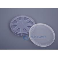
N Type , Vgf GaAs (Gallium Arsenide) Wafer ,2”, Test Grade -Wafer Manufacturing
PAM-XIAMEN develops and manufactures compound semiconductor substrates-gallium arsenide crystal and wafer.We has used advanced crystal growth technology,vertical gradient freeze(VGF) and GaAs wafer processing technology,established a production line from crystal growth, cutting, grinding to polishing processing and built a 100-class clean room for wafer cleaning and packaging. Our GaAs wafer include 2~6 inch ingot/wafers for LED,LD and Microelectronics applications. We are always dedicated to improve the quality of currently substates and develop large size substrates.
(GaAs)Gallium Arsenide Wafers for LED Applications
| Item | Specifications | |
| Conduction Type | SC/n-type | |
| Growth Method | VGF | |
| Dopant | Silicon | |
| Wafer Diamter | 2, inch | |
| Crystal Orientation | (100)2°/6°/15° off (110) | |
| OF | EJ or US | |
| Carrier Concentration | (0.4~2.5)E18/cm3
| |
| Resistivity at RT | (1.5~9)E-3 Ohm.cm | |
| Mobility | 1500~3000cm2/V.sec
| |
| Etch Pit Density | <5000/cm2 | |
| Laser Marking | upon request
| |
| Surface Finish | P/E or P/P
| |
| Thickness | 220~450um
| |
| Epitaxy Ready | Yes | |
| Package | Single wafer container or cassette | |
(GaAs)Gallium Arsenide Wafers for LD Applications
| Item | Specifications | Remarks |
| Conduction Type | SC/n-type | |
| Growth Method | VGF | |
| Dopant | Silicon | |
| Wafer Diamter | 2, inch | Ingot or as-cut available |
| Crystal Orientation | (100)2°/6°/15°off (110) | Other misorientation available |
| OF | EJ or US | |
| Carrier Concentration | (0.4~2.5)E18/cm3 | |
| Resistivity at RT | (1.5~9)E-3 Ohm.cm | |
| Mobility | 1500~3000 cm2/V.sec | |
| Etch Pit Density | <500/cm2 | |
| Laser Marking | upon request | |
| Surface Finish | P/E or P/P | |
| Thickness | 220~350um | |
| Epitaxy Ready | Yes | |
| Package | Single wafer container or cassette | |
Properties of GaAs Crystal
| Properties | GaAs |
| Atoms/cm3 | 4.42 x 10²² |
| Atomic Weight | 144.63 |
| Breakdown Field | approx. 4 x 10⁵ |
| Crystal Structure | Zincblende |
| Density (g/cm3) | 5.32 |
| Dielectric Constant | 13.1 |
| Effective Density of States in the Conduction Band, Nc (cm-3) | 4.7 x 10¹⁷ |
| Effective Density of States in the Valence Band, Nv (cm-3) | 7.0 x 10¹⁸ |
| Electron Affinity (V) | 4.07 |
| Energy Gap at 300K (eV) | 1.424 |
| Intrinsic Carrier Concentration (cm-3) | 1.79 x 10⁶ |
| Intrinsic Debye Length (microns) | 2250 |
| Intrinsic Resistivity (ohm-cm) | 108 |
| Lattice Constant (angstroms) | 5.6533 |
| Linear Coefficient of Thermal Expansion, | 6.86 x 10⁻⁶ |
| ΔL/L/ΔT (1/deg C) | |
| Melting Point (deg C) | 1238 |
| Minority Carrier Lifetime (s) | approx. 10-8 |
| Mobility (Drift) | 8500 |
| (cm2/V-s) | |
| µn, electrons | |
| Mobility (Drift) | 400 |
| (cm2/V-s) | |
| µp, holes | |
| Optical Phonon Energy (eV) | 0.035 |
| Phonon Mean Free Path (angstroms) | 58 |
| Specific Heat | 0.35 |
| (J/g-deg C) | |
| Thermal Conductivity at 300 K | 0.46 |
| (W/cm-degC) | |
| Thermal Diffusivity (cm2/sec) | 0.24 |
| Vapor Pressure (Pa) | 100 at 1050 deg C; |
| 1 at 900 deg C |
| Wavelength | Index |
| (µm) | |
| 2.6 | 3.3239 |
| 2.8 | 3.3204 |
| 3 | 3.3169 |
| 3.2 | 3.3149 |
| 3.4 | 3.3129 |
| 3.6 | 3.3109 |
| 3.8 | 3.3089 |
| 4 | 3.3069 |
| 4.2 | 3.3057 |
| 4.4 | 3.3045 |
| 4.6 | 3.3034 |
| 4.8 | 3.3022 |
| 5 | 3.301 |
| 5.2 | 3.3001 |
| 5.4 | 3.2991 |
| 5.6 | 3.2982 |
| 5.8 | 3.2972 |
| 6 | 3.2963 |
| 6.2 | 3.2955 |
| 6.4 | 3.2947 |
| 6.6 | 3.2939 |
| 6.8 | 3.2931 |
| 7 | 3.2923 |
| 7.2 | 3.2914 |
| 7.4 | 3.2905 |
| 7.6 | 3.2896 |
| 7.8 | 3.2887 |
| 8 | 3.2878 |
| 8.2 | 3.2868 |
| 8.4 | 3.2859 |
| 8.6 | 3.2849 |
| 8.8 | 3.284 |
| 9 | 3.283 |
| 9.2 | 3.2818 |
| 9.4 | 3.2806 |
| 9.6 | 3.2794 |
| 9.8 | 3.2782 |
| 10 | 3.277 |
| 10.2 | 3.2761 |
| 10.4 | 3.2752 |
| 10.6 | 3.2743 |
| 10.8 | 3.2734 |
| 11 | 3.2725 |
| 11.2 | 3.2713 |
| 11.4 | 3.2701 |
| 11.6 | 3.269 |
| 11.8 | 3.2678 |
| 12 | 3.2666 |
| 12.2 | 3.2651 |
| 12.4 | 3.2635 |
| 12.6 | 3.262 |
| 12.8 | 3.2604 |
| 13 | 3.2589 |
| 13.2 | 3.2573 |
| 13.4 | 3.2557 |
| 13.6 | 3.2541 |
What is a GaAs Test Wafer?
Most GaAs test wafers are wafers which have fallen out of prime specifications. Test wafers may be used to run marathons, test equipment and for high-end R & D. They are often a cost-effective alternative to prime wafers.
| Breakdown field | ≈4·105 V/cm |
| Mobility electrons | ≤8500 cm2 V-1s-1 |
| Mobility holes | ≤400 cm2 V-1s-1 |
| Diffusion coefficient electrons | ≤200 cm2/s |
| Diffusion coefficient holes | ≤10 cm2/s |
| Electron thermal velocity | 4.4·105 m/s |
| Hole thermal velocity | 1.8·105m/s |
Mobility and Hall Effect
| Electron Hall mobility versus temperature for different doping
levels. 1. Bottom curve: Nd=5·1015cm-3; 2. Middle curve : Nd=1015cm-3; 3. Top curve : Nd=5·1015cm-3 For weakly doped GaAs at temperature close to 300 K, electron Hall mobility µH=9400(300/T) cm2 V-1 s-1 |
| Electron Hall mobility versus temperature for different doping
levels and degrees of compensation (high temperatures): Open circles: Nd=4Na=1.2·1017 cm-3; Open squares: Nd=4Na=1016 cm-3; Open triangles: Nd=3Na=2·1015 cm-3; Solid curve represents the calculation for pure GaAs For weakly doped GaAs at temperature close to 300 K, electron drift mobility µn=8000(300/T)2/3 cm2 V-1 s-1 |
| Drift and Hall mobility versus electron concentration for different
degrees of compensation T= 77 K |
| Drift and Hall mobility versus electron concentration for different
degrees of compensation T= 300 K |
Approximate formula for the Hall mobility
. µn =µOH/(1+Nd·10-17)1/2, where µOH≈9400 (cm2 V-1 s-1), Nd- in
cm-3
| Temperature dependence of the Hall factor for pure n-type GaAs in a
weak magnetic field |
| Temperature dependence of the Hall mobility for three high-purity
samples |
For GaAs at temperatures close to 300 K, hole Hall mobility
 (cm2V-1s-1), (p - in cm-3)
For weakly doped GaAs at temperature close to 300 K, Hall mobility
µpH=400(300/T)2.3 (cm2 V-1 s-1).
| The hole Hall mobility versus hole density. |
At T= 300 K, the Hall factor in pure GaAs
rH=1.25.
Transport Properties in High Electric Fields
| Field dependences of the electron drift velocity. Solid curve was calculated by. Dashed and dotted curves are measured data, 300 K |
| Field dependences of the electron drift velocity for high electric
fields, 300 K. |
| Field dependences of the electron drift velocity at different
temperatures. |
| Fraction of electrons in L and X valleys. nL and nX as a function
of electric field F at 77, 160, and 300 K, Nd=0 Dotted curve - L valleys, dashed curve - X valleys. |
| Mean energy E in Γ, L, and X valleys as a function of electric
field F at 77, 160, and 300 K, Nd=0 Solid curve - Γ valleys, dotted curve - L valleys, dashed curve - X valleys. |
| Frequency dependences of electron differential mobility. µd is real part of the differential mobility; µd*is imaginary part of differential mobility. F= 5.5 kV cm-1 |
| The field dependence of longitudinal electron diffusion coefficient
D||F. Solid curves 1 and 2 are theoretical calculations. Dashed curves 3, 4, and 5 are experimental data. Curve 1 - from Curve 2 - from Curve 3 - from Curve 4 - from Curve 5 - |
| Field dependences of the hole drift velocity at different
temperatures. |
| Temperature dependence of the saturation hole velocity in high
electric fields |
| The field dependence of the hole diffusion coefficient. |
Impact Ionization
There are two schools of thought regarding the impact ionization in GaAs.
The first one states that impact ionization rates αi and βi for electrons and holes in GaAs are known accurately enough to distinguish such subtle details such as the anisothropy of αi and βi for different crystallographic directions. This approach is described in detail in the work by Dmitriev et al.[1987].
| Experimental curves αi and βi versus 1/F for GaAs. |
| Experimental curves αi and βi versus 1/F for GaAs. |
| Experimental curves αi and βi versus 1/F for GaAs. |
The second school focuses on the values of αi and βi for the same
electric field reported by different researches differ by an order
of magnitude or more. This point of view is explained by Kyuregyan
and Yurkov [1989]. According to this approach we can assume that αi
= βi. Approximate formula for the field dependence of ionization
rates:
αi = β i =αoexp[δ - (δ2 + (F0 / F)2)1/2]
where αo = 0.245·106 cm-1; β = 57.6 Fo = 6.65·106 V cm-1 (Kyuregyan
and Yurkov [1989]).
| Breakdown voltage and breakdown field versus doping density for an
abrupt p-n junction. |
Recombination Parameter
| Pure n-type material (no ~ 1014cm-3) | |
| The longest lifetime of holes | τp ~3·10-6 s |
| Diffusion length Lp = (Dp·τp)1/2 | Lp ~30-50 µm. |
| Pure p-type material | |
| (a)Low injection level | |
| The longest lifetime of electrons | τn ~ 5·10-9 s |
| Diffusion length Ln = (Dn·τ n)1/2 | Ln ~10 µm |
| (b) High injection level (filled traps) | |
| The longest lifetime of electrons | τ ~2.5·10-7 s |
| Diffusion length Ln | Ln ~ 70 µm |
| Surface recombination velocity versus doping density Different experimental points correspond to different surface treatment methods. |
Radiative recombination coefficient
| 90 K | 1.8·10-8cm3/s |
| 185 K | 1.9·10-9cm3/s |
| 300 K | 7.2·10-10cm3/s |
Auger coefficient
| 300 K | ~10-30cm6/s |
| 500 K | ~10-29cm6/s |
Are You Looking for GaAs substrate?
PAM-XIAMEN is proud to offer indium phosphide substrate for all different kinds of projects. If you are looking for GaAs wafers, send us enquiry today to learn more about how we can work with you to get you the GaAs wafers you need for your next project. Our group team is looking forward to providing both quality products and excellent service for you!
 Wafer ,2”, Test Grade -Wafer Manufacturing")
 Wafer ,2”, Test Grade -Wafer Manufacturing")
 Wafer ,2”, Test Grade -Wafer Manufacturing")
 Wafer ,2”, Test Grade -Wafer Manufacturing")
 Wafer ,2”, Test Grade -Wafer Manufacturing")
 Wafer ,2”, Test Grade -Wafer Manufacturing")