|
|
[China]

Trade Verify
Address: Rm5-616,No.851,Dianshanhu avenue, Qingpu area,Shanghai city,CHINA
Contact name:Wang

SHANGHAI FAMOUS TRADE CO.,LTD |
|
Verified Suppliers
|

|
|
4inch 6inch GaN-ON-SiC EPI layer wafers GaN-ON-Si EPI layer wafers
About GaN-on-GaN GaN-on-SIC Feature Introduce
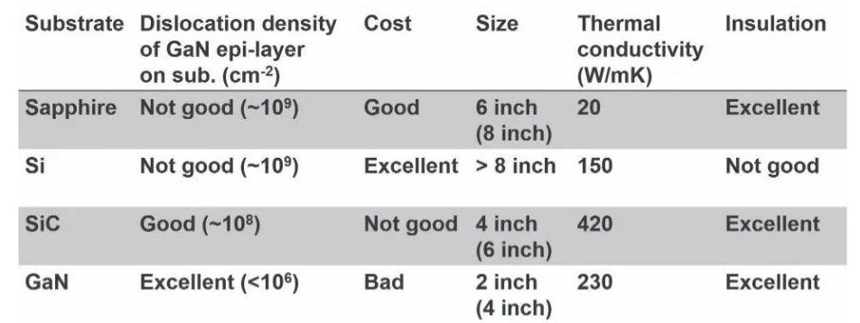
GaN epitaxial wafer: According to the different substrates, it is
mainly divided into four types: GaN-on-Si, GaN-on-SiC,
GaN-on-sapphire, and GaN-on-GaN.
GaN-on-Si: The current industry production yield is
low, but there is a huge potential for cost reduction: because Si
is the most mature, defect-free, and lowest-cost substrate
material; at the same time, Si can be expanded to 8-inch wafer fabs
, reduce the unit production cost, so that the wafer cost is only
one percent of that of the SiC base; the growth rate of Si is 200
to 300 times that of the SiC crystal material, and the
corresponding fab equipment depreciation and energy consumption
difference in cost, etc. GaN-on-Si epitaxial wafers are mainly used
in the manufacture of power electronic devices, and the technical
trend is to optimize large-scale epitaxy technology.
GaN-on-SiC: Combining the excellent thermal
conductivity of SiC with the high power density and low loss
capabilities of GaN, it is a suitable material for RF. Limited by
the SiC substrate, the current size is still limited to 4 inches
and 6 inches, and 8 inches has not been promoted. GaN-on-SiC
epitaxial wafers are mainly used to manufacture microwave radio
frequency devices.
GaN-on-sapphire: Mainly used in the LED market, the mainstream size is 4 inches, and the market share of GaN LED chips on sapphire substrates has reached more than 90%.
GaN-on-GaN: The main application market of GaN
using homogenous substrates is blue/green lasers, which are used in
laser display, laser storage, laser lighting and other fields.
GaN device design and manufacturing: GaN
devices are divided into radio frequency devices and power
electronic devices. Radio frequency device products include PA,
LNA, switches, MMICs, etc., which are oriented to base station
satellite, radar and other markets; power electronic device
products include SBD, normally-off FET. , Normally-on FET, Cascode
FET and other products for wireless charging, power switch,
envelope tracking, inverter, converter and other markets.
According to the process, it is divided into two categories: HEMT,
HBT radio frequency process and SBD, PowerFET power electronic
device process.
Applications
Specifications for GaN-on-GaN Substrates for Each Grade
| 4-6”GaN ON-SIC |
| Item | Type: N-type SIC |
| Dimensions size | Ф 100.0mm ± 0.5mm |
| Thickness of Substrate | 350 ± 30 µm |
| Orientation of Substrate | 4°off C-axis(0001) |
| Polish | DSP |
| Ra | <0.2nm |
| Epilyaer structure | 0.5um pGaN/20um iGaN/2um nGaN/FS-GaN |
| Epi thickness/STD | 1~25um/<3% |
| Roughness | <0.5nm |
| Discolation density | <1X107cm-2 |
| pGaN Carrier concentration | >1E17CM-3; |
| iGaN Carrier concentration | > 1E17CM-3; |
| nGaN Carrier concentration | >1E17CM-3; |
| Useable area | P level>90%; R level>80%: Dlevel>70%(edge and macro defects exclusion) |

Our services
1. Factory direct manufacture and sell.
2. Fast, accurate quotes.
3. Reply to you within 24 working hours.
4. ODM: Customized design is avaliable.
5. Speed and precious delivery.
FAQ
Q: Is there any stock or standard product?
A: Yes, commen size as like2inch 0.3mm standard size always in stocks.
Q: How about the samples policy?
A: sorry, but suggest you can buy some 10x10mm size back for test firstly.
Q: If i place an order now ,how long would it be before i got delivery ?
A: standard size in stock in 1weeks can be expressed after payment.
and our payment term is 50% deposit and left before delivery.