
|
|
[China]

Trade Verify
Address: Rm5-616,No.851,Dianshanhu avenue, Qingpu area,Shanghai city,CHINA
Contact name:Wang

SHANGHAI FAMOUS TRADE CO.,LTD |
|
Verified Suppliers
|
|
|
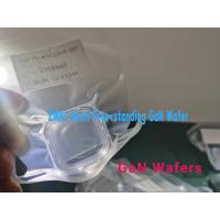
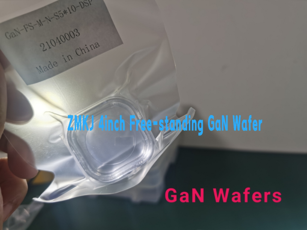
2inch free-standing GaN substrates,GaN wafer for LD, semiconducting Gallium Nitride Wafer for led,GaN template,10x10mm GaN substrates, native GaN wafer,
GaN Applications
GaN can be used to make several types of devices; the primary GaN devices are LEDs, laser diodes, power electronics, and RF devices.
GaN is ideal for LEDs because of the direct bandgap of 3.4 eV which is in the near UV spectrum. GaN can be alloyed with InN and AlN, which have bandgaps of 0.7 eV and 6.2 eV, respectively. Therefore, this material systems can theoretically span a large energy spectrum for light emitting device. In actual practice, the efficiency is highest for blue InGaN devices and decreases for high indium content InGaN or for AlGaN emitters. The near UV and blue spectrum is optimal for making white emitters with phosphors, and this technology has been responsible for the remarkable efficiency gains in lighting since the 1990s when LEDs have begun to replace traditional light sources.
Laser diodes, usually with blue emission, can be made using GaN. These devices are used for displays and some specialty biomedical, cutting, and scientific applications. Laser diodes can also be used for making white light emitting devices with phosphors. Compared to LEDs, laser diode white light can achieve a very high power density and high directionality.
For power electronics, GaN-based devices can achieve high switching speeds, high power density, and low energy losses resulting in more efficient, smaller, and lighter power conversion products. There are numerous applications for GaN-based power electronics including electric vehicles, solar and wind energy inverters, industrial motor controllers, data centers, and consumer electronics.
GaN-based RF devices possess many of the same advantages of GaN power electronics, and additionally can access higher frequency than traditional semiconductors. RF devices are used for industrial heating, radar, and telecommunications. GaN is especially advantageous for high power density such as for cellular base stations.
HVPE Technology
Hydride Vapor Phase Epitaxy (HVPE) is a process that can produce single crystal GaN. It is used for the growth of GaN substrates because of the high growth rate and high quality that can be attained. In this process, HCl gas is reacted with liquid gallium metal, which forms GaCl gas. Then the GaCl reacts with NH₃ gas at about 1,000 °C to form the solid crystal of GaN. Eta Research has developed our own HVPE equipment with the goal to cost effectively scale the production of GaN wafers.
Presently, the vast majority of GaN-based devices use foreign substrates such as Al₂O₃ and Si. Although foreign substrates are good for some applications, the dissimilar material causes defects to be placed in the GaN device layers as material is deposited. The defects can reduce the performance.
GaN substrates, especially with low defect density, offer the best choice for deposition of GaN device layers. Use of GaN substrates will improve the efficiency, power density, and other performance metrics of GaN devices.
Specifications:
| Item | GaN-FS-N | |
| Dimensions | Ф 100mm ± 1mm | |
| Marco Defect Density | A Level | ≤ 2 cm-2 |
| B Level | > 2 cm-2 | |
| Thickness | 450 ± 25 µm | |
| Orientation | C-axis(0001) ± 0.5° | |
| Orientation Flat | (1-100) ± 0.5°, 32.0 ± 1.0mm | |
| Secondary Orientation Flat | (11-20) ± 3°, 18.0 ± 1.0mm | |
| TTV(Total Thickness Variation) | ≤30 µm | |
| BOW | ≤30 µm | |
| Conduction Type | N-type | |
| Resistivity(300K) | < 0.5 Ω·cm | |
| Dislocation Density | Less than 5x106 cm-2 | |
| Useable Surface Area | > 90% | |
| Polishing | Front Surface: Ra < 0.2nm. Epi-ready polished Back Surface: Fine ground | |
| Package | Packaged in a class 100 clean room environment, in single wafer containers, under a nitrogen atmosphere. | |
or by customzied size

2. Our Enterprise Vision
we will provide high quality GaN substrate and application technology for the industry.
High quality GaNmaterial is the restraining factor for the III-nitrides application, e.g. long life and high stability LDs, high power and high reliability micro-wave devices, High brightness and high efficiency, energy-saving LED.
-FAQ –
Q: What you can supply logistics and cost?
(1) We accept DHL, Fedex, TNT, UPS, EMS, SF and etc.
(2) If you have your own express number, it's great.
If not, we could assist you to deliver. Freight=USD25.0(the first
weight) + USD12.0/kg
Q: What's the delivery time?
(1) For the standard products such as 2inch 0.33mm wafer.
For inventory: the delivery is 5 workdays after order.
For customized products: the delivery is 2 or 3 workweeks after
order.
Q: How to pay?
100%T/T, Paypal, West Union, MoneyGram, Secure payment and Trade
Assurance.
Q: What's the MOQ?
(1) For inventory, the MOQ is 1pcs.
(2) For customized products, the MOQ is 5pcs-10pcs.
It depends on quantity and technics.
Q: Do you have inspection report for material?
We can supply ROHS report and reach reports for our products.


