
|
|
[China]

Trade Verify
Address: Rm5-616,No.851,Dianshanhu avenue, Qingpu area,Shanghai city,CHINA
Contact name:Wang

SHANGHAI FAMOUS TRADE CO.,LTD |
|
Verified Suppliers
|
|
|
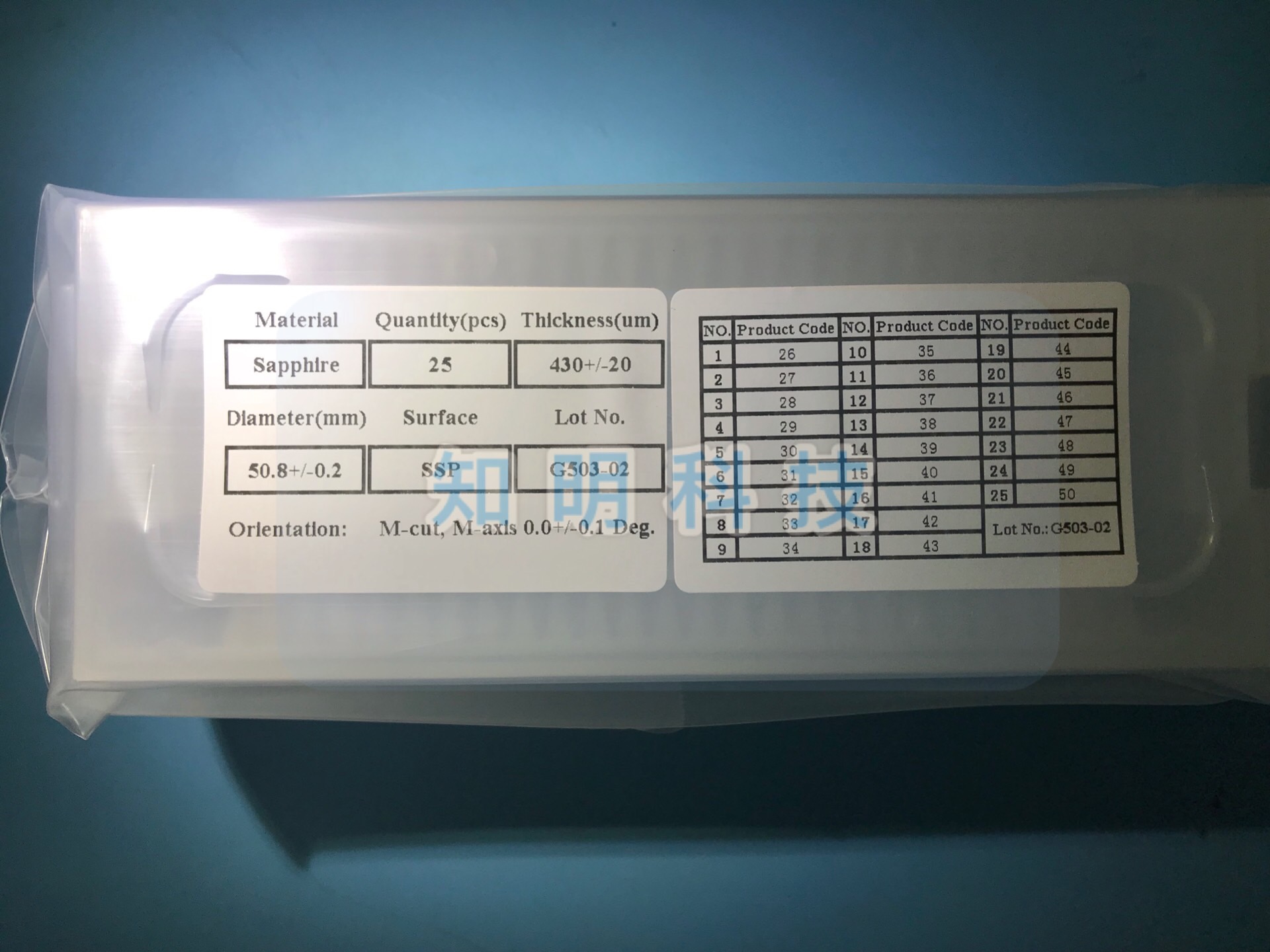
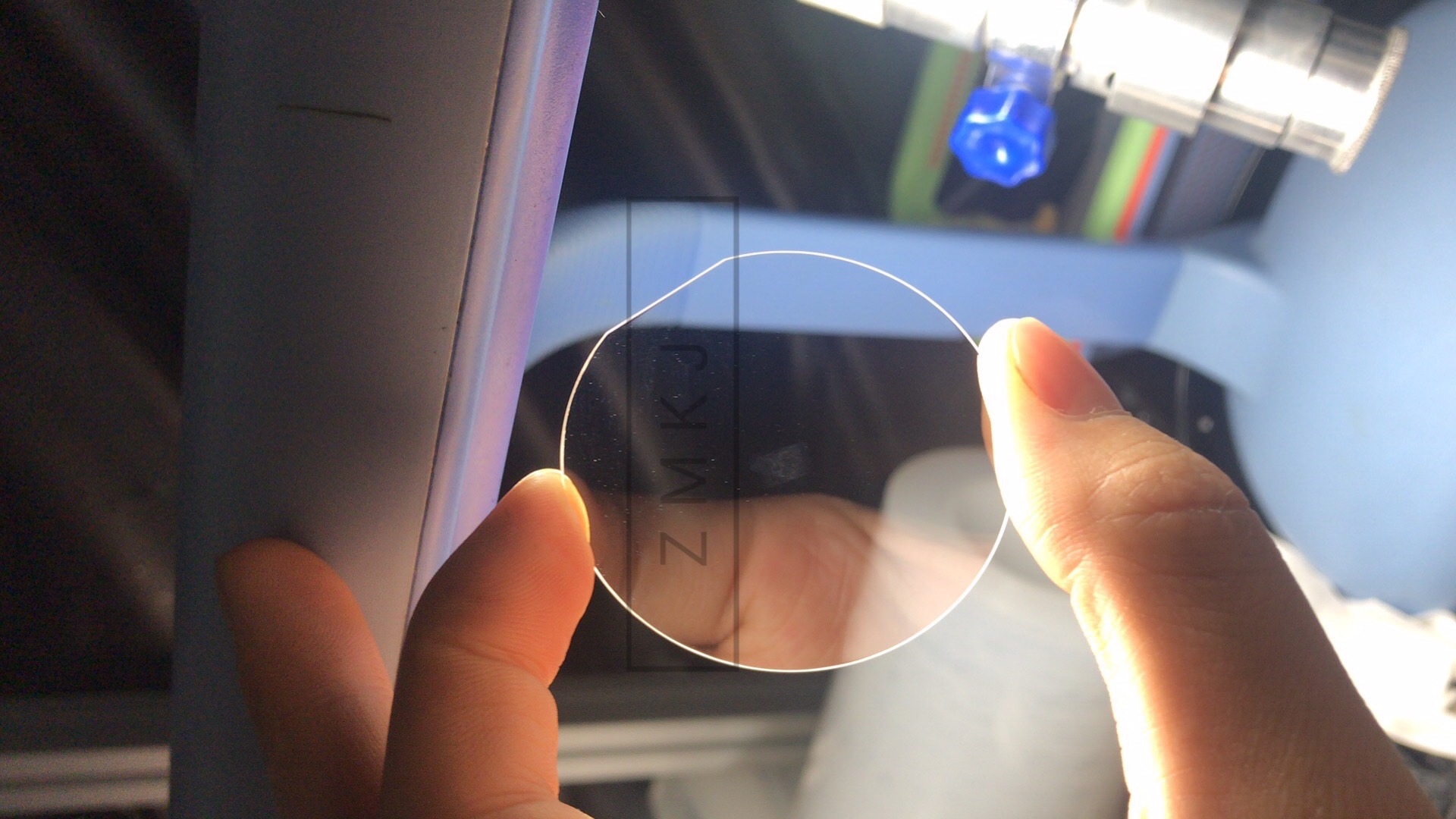
2inch M-axis 0.5mm thickness sapphire wafer for epi-ready test
,sapphire optical windows, M-axis 2inch sapphire epi-ready
substrate
1. Description
Sapphire is one of the hardest materials, and possesses very good
transmission during the range of visible and near IR spectrum.It is
widely used as optical window in infrared and far infrared military
equipments, apparatus and instruments of satellite and space
technology, and navigation and spaceflight, such as night infrared
scope/sight and night vision camera, etc.The sapphire crystal
window is intensively applied in high-tech fields.
Sapphire optical windows are ideal for applications where high
pressure, vacuum, or corrosive atmospheres are a consideration.
Sapphire, a single crystal form of Al2O3, is resistant to attack by
strong acids due to its high dielectric constant. It has high
compressive strength and a high melting point. It is also resistant
to UV radiation darkening.
sapphire application: sapphire optical lens ,sapphire ball,
sapphire bearing ,sapphire led wafer, sapphire watch glass lens.
Specification:

2. QC Standard


3. FAQ:
1. Can you accept OEM?
Yes!above thickness 0.5mm wafers are OEM products
2. Can you deliver the goods via our shipping agent?
Yes, we could help you make the delivery using your shipping agent
3. What about your After-sales service?
Yes.We promise that we can change or refund products if there are
any quality problem.
4.How about the delivery date?
commenly we have some standard size on stock as like 2inch R-axis, M-axis,A-axis ,C-axis
by thickness 0.43mm DSP and SSP. please understand~
if customized specifications in 4weeks.
If you need more professional help, please contact us. Our technical engineers
would like to give advices according to your requirements
we also provide other materials semiconductor wafer as likes SiC, GaN, GaAs, InP .


