
|
|
[China]

Trade Verify
Address: Rm5-616,No.851,Dianshanhu avenue, Qingpu area,Shanghai city,CHINA
Contact name:Wang

SHANGHAI FAMOUS TRADE CO.,LTD |
|
Verified Suppliers
|
|
|
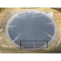
6inch sic substrates, sic ingot sic crystal ingots sic crystal block sic semiconductor substrates 2inch 3inch 4inch 6inch 4h no doped wafer
we can provides high quality single crystal SiC wafer ( Silicon Carbide ) to electronic and optoelectronic industry . SiC wafer is a next generation semiconductor material , with unique electrical properties and excellent thermal properties , compared to silicon wafer and GaAs wafer , SiC wafer is more suitable for high temperature and high power device application . SiC wafer can be supplied in diameter 2 -6inch , both 4H and 6H SiC , N-type , Nitrogen doped , and semi-insulating type available . Please contact us for more product information .
1.material application and advantagement
Applications:
• GaN epitaxy device
• Optoelectronic device
• High frequency device
• High power device
• High temperature device
• Light emitting diodes
• Low lattice mismatch
• High thermal conductivity
• Low power consumption
• Excellent transient characteristics
• High band gap
SILICON CARBIDE MATERIAL PROPERTIES | ||
Polytype | Single Crystal 4H | Single Crystal 6H |
Lattice Parameters | a=3.076 Å | a=3.073 Å |
c=10.053 Å | c=15.117 Å | |
Stacking Sequence | ABCB | ABCACB |
Band-gap | 3.26 eV | 3.03 eV |
Density | 3.21 · 103 kg/m3 | 3.21 · 103 kg/m3 |
Therm. Expansion Coefficient | 4-5×10⁻⁶/K | 4-5×10⁻⁶/K |
Refraction Index | no = 2.719 | no = 2.707 |
ne = 2.777 | ne = 2.755 | |
Dielectric Constant | 9.6 | 9.66 |
Thermal Conductivity | 490 W/mK | 490 W/mK |
Break-Down Electrical Field | 2 – 4 · 108 V/m | 2 – 4 · 108 V/m |
Saturation Drift Velocity | 2.0 · 105 m/s | 2.0 · 105 m/s |
Electron Mobility | 800 cm2/V·S | 400 cm2/V·S |
hole Mobility | 115 cm2/V·S | 90 cm2/V·S |
Mohs Hardness | ~9 | |


FAQ:
Q: What's your MOQ and delivery time?
A: (1) For inventory, the MOQ is 3pcs. if 5-10pcs it's better in 10-30days
(2) For 6inch customized products, the MOQ is 10pcs up in 30-50days
Q: What's the way of shipping and cost?
A:(1) We accept DHL, Fedex, EMS etc.
(2) it is fine If you have your own express account ,If not,we could help you ship them and Freight is in accordance with the actual settlement.
Q: How to pay?
A: T/T, 100%
Q: Do you have standard products?
A:there are not 6inch Our standard products in stock.
but as like substrates 4inch 0.33mm 2sp thickness have some in stock


