
|
|
[China]

Trade Verify
Address: Rm5-616,No.851,Dianshanhu avenue, Qingpu area,Shanghai city,CHINA
Contact name:Wang

SHANGHAI FAMOUS TRADE CO.,LTD |
|
Verified Suppliers
|
|
|
2inch GaN substrates template,GaN wafer for LeD,semiconducting
Gallium Nitride Wafer for ld,GaN template, mocvd GaN
Wafer,Free-standing GaN Substrates by Customized size,small size
GaN wafer for LED, mocvd Gallium Nitride wafer 10x10mm,5x5mm,
10x5mm GaN wafer
Gallium Nitride is one kind of wide-gap compound semiconductors. Gallium Nitride (GaN) substrate is
a high-quality single-crystal substrate. It is made with original HVPE method and wafer processing technology, which has been originally developed for 10+years in China. The features are high crystalline, good uniformity, and superior surface quality. GaN substrates are used for many kinds of applications, for white LED and LD(violet, blue and green) Furthermore, development has progressed for power and high frequency electronic device applications.
Forbidden band width (light emitting and absorption)
cover the ultraviolet, visible light and infrared.
GaN can be used in many areas such as LED display, High-energy
Detection and Imaging,
Specifications:
| Free-standing GaN Substrates (Customized size) | ||
| Item | GaN-FS-10 | GaN-FS-15 |
| Dimensions | 10.0mm×10.5mm | 14.0mm×15.0mm |
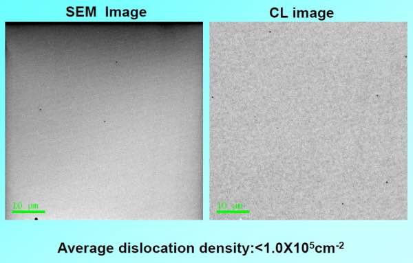
| Marco Defect Density | A Level | 0 cm-2 |
| B Level | ≤ 2 cm-2 | |
| Thickness | Rank 300 | 300 ± 25 µm |
| Rank 350 | 350 ± 25 µm | |
| Rank 400 | 400 ± 25 µm | |
| Orientation | C-axis(0001) ± 0.5° | |
| TTV ( Total Thickness Variation) | ≤15 µm | |
| BOW | ≤20 µm | |
| Conduction Type | N-type | Semi-Insulating |
| Resistivity(300K) | < 0.5 Ω·cm | >106 Ω·cm |
| Dislocation Density | Less than 5x106 cm-2 | |
| Useable Surface Area | > 90% | |
| Polishing | Front Surface: Ra < 0.2nm. Epi-ready polished | |
| Back Surface: Fine ground | ||
| Package | Packaged in a class 100 clean room environment, in single wafer containers, under a nitrogen atmosphere. | |

| Item | GaN-FS-N-1.5 | |||
| Dimensions | Ф 25.4mm ± 0.5mm | Ф 38.1mm ± 0.5mm | Ф 40.0mm ± 0.5mm | Ф 45.0mm ± 0.5mm |
| Marco Defect Density | A Level | ≤ 2 cm-2 | ||
| B Level | > 2 cm-2 | |||
| Thickness | 300 ± 25 µm | |||
| Orientation | C-axis(0001) ± 0.5° | |||
| Orientation Flat | (1-100) ± 0.5° | (1-100) ± 0.5° | (1-100) ± 0.5° | (1-100) ± 0.5° |
| 8 ± 1mm | 12 ± 1mm | 14 ± 1mm | 14 ± 1mm | |
| Secondary Orientation Flat | (11-20) ± 3° | (11-20) ± 3° | (11-20) ± 3° | (11-20) ± 3° |
| 4 ± 1mm | 6 ± 1mm | 7 ± 1mm | 7 ± 1mm | |
| TTV(Total Thickness Variation) | ≤15 µm | |||
| BOW | ≤20 µm | |||
| Conduction Type | N-type | Semi-Insulating | ||
| Resistivity(300K) | < 0.5 Ω·cm | >106 Ω·cm | ||
| Dislocation Density | Less than 5x106 cm-2 | |||
| Useable Surface Area | > 90% | |||
| Polishing | Front Surface: Ra < 0.2nm. Epi-ready polished | |||
| Back Surface: Fine ground | ||||
| Package | Packaged in a class 100 clean room environment, in single wafer containers, under a nitrogen atmosphere. | |||

Our Factroy Enterprise Vision
we will provide high quality GaN substrate and application
technology for the industry with our factory.
High quality GaNmaterial is the restraining factor for the
III-nitrides application, e.g. long life
and high stability LDs, high power and high reliability micro-wave
devices, High brightness
and high efficiency, energy-saving LED.
-FAQ –
Q: What you can supply logistics and cost?
(1) We accept DHL, Fedex, TNT, UPS, EMS, SF and etc.
(2) If you have your own express number, it's great.
If not, we could assist you to deliver. Freight=USD25.0(the first
weight) + USD12.0/kg
Q: What's the delivery time?
(1) For the standard products such as 2inch 0.33mm wafer.
For inventory: the delivery is 5 workdays after order.
For customized products: the delivery is 2 or 4 workweeks
after order.
Q: How to pay?
100%T/T, Paypal, West Union, MoneyGram, Secure payment and Trade
Assurance.
Q: What's the MOQ?
(1) For inventory, the MOQ is 5pcs.
(2) For customized products, the MOQ is 5pcs-10pcs.
It depends on quantity and technics.
Q: Do you have inspection report for material?
We can supply ROHS report and reach reports for our products.


