
|
|
[China]

Trade Verify
Address: Rm5-616,No.851,Dianshanhu avenue, Qingpu area,Shanghai city,CHINA
Contact name:Wang

SHANGHAI FAMOUS TRADE CO.,LTD |
|
Verified Suppliers
|
|
|
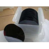
8inch sillicon wafer sillicon optical lens IC sillicon substrates sillicon ingots poly sillicon wafer
1. Specification
| Diameter (mm) | 50.8 | 76.2 | 100 | 125 | 150 | 200 |
| Growth Method | MCZ | |||||
| Type Dopant | N: Arsenic / Antimony / Phosphorus/Red Phos | |||||
| P: Boron | ||||||
| Resistivity (Ω.cm)* | MCZ: 1 × 10⁻³ ~ 100 | |||||
| Thickness (μm)* | 381 | 381 | 525 | 525 | 675 | 725 |
| Thickness Tolerance (μm) | Typical ± 25 | |||||
| TTV (μm) | 10 | |||||
| Bow (μm) | 30 | 30 | 40 | 40 | 40 | 60 |
* Other surface conditions & customized specifications are
welcome Backside Seal LTO & Poly both are available Other unmentioned parameters are per Semi Standard | ||||||
CZ 8inch dummy wafer, test wafer for semiconductor process
Diameter : 200 +/- 0.5 mm ; 200 +/- 0.2 mm
Type / Dopant : P/Boron
Orientation ; <100> +/- 1º
Grade : Test ; Prime
Resistivity : 1 - 100 Ω-cm ; 8 - 12 Ω-cm
Radial Resisivity Gradient: — As Specified
Oxygen :— As Specified
Carbon :— As Specified
Metals : < 5 x E10 atoms/cm2
Thickness : 725 +/- 25 μm ; 725 +/- 15 μm
TTV : <= 10 μm ; <= 5 μm
GTIR : <= 2 μm
Bow / Warp : <= 50 μm ; <= 40 μm
STIR :— <= 2 μm
Flats:SEMI Standard
Particle Count : <= 30 @ >= 0.2 μm ; <= 50 @ >= 0.09 μm
Polished : Single Side Polished or Double Side Polished
Etched : Single Side Polished or Double Side Polished
* N type wafers available

About wafer process
crystal growth body--->crystal cutting by wire saw----->spheronizations
----->annealing------>engraving number--->lapped &polished---> Testing
FAQ:
Q: What's the way of shipping and cost?
A:(1) We accept DHL, Fedex, EMS etc.
(2) If you have your own express account, it's great.If not,we could help you ship them.
Freight is in accordance with the actual settlement.
Q: How to pay?
A: T/T, Paypal, Secure payment and Assurance payment.
Q: What's your MOQ?
A: (1) For inventory, the MOQ is 25pcs.
(2) For customized products, the MOQ is 25pcs up.
Q: What's the delivery time?
A: (1) For the standard products
For inventory: the delivery is 5 workdays after you place the order.
For customized products: the delivery is 2 or 3 weeks after you place the order.
(2) For the special-shaped products, the delivery is 4 workweeks after you place the order.
Q: Do you have standard products?
A: Our standard products in stock.
Q: Can I customize the products based on my need?
A: Yes, we can customize the material, specifications and optical coating for your optical components
based on your needs.


