

Active Member
|
[China]

Address: Room 403 Block A,Huafeng SOHO Creative World Hangcheng Industrial Zone Qianjin 2nd Road,Xixiang Baoan Shenzhen,China
Contact name:karen

Shenzhen Xinchenger Electronic Co.,Ltd |
|
|
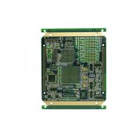
High desity PCB16 Layer High TG ENIG PCB
Layer: 16
Surface Finish: ENIG
Material: High TG FR4
Outer Track W/S: 4/4mil
Inner Track W/S: 3.5/3.5mil
Board Thickness: 2.43mm
Min. Hole Diameter: 0.75mm
Application Industry: Industrial Control
Application Products: Function Board
HDI PCB is among the fastest growing PCBs on the market because it meets complex design needs. This kind of high density interconnect printed circuit board allows designers to place more components in a smaller area. Having a higher circuitry density than conventional PCBs, it's able to incorporate finer lines and spaces, smaller vias & capture pads, and higher connection pad densities. It contains blind/buried vias and is often with 6 mil microvias.
HDI custom PCB is widely used to reduce the weight and overall dimensions of products, as well as enhancing the electrical performance of the device. It's regularly found in mobile phones, touch-screen devices, and 4G network communications.
XCEPCB offers HDI custom PCB fabrication with microvias down to 4 mil; laser drilling is required.
| HDI Structures | Type of micorovias | Mass production | Middle/small batch | Prototype | Apply to |
| 1+N+1 | Blind vias | Yes | Yes | Yes | 4 layers+ |
| 2+N+2 | Blind/Buried staggered vias | Yes | Yes | Yes | 6 layers+ |
| 2+N+2 | Blind/Buried stacked vias | Yes | Yes | Yes | 6 layers+ |
| 3+N+3 | Blind/Buried staggered vias | / | Yes | Yes | 8 layers+ |
| 3+N+3 | Blind/Buried stacked vias | / | / | Yes | 8 layers+ |
Our PCB Application:
We can offer production with high quality and competitive:
| Item | Mass Production | Pilot Run Production |
| Capacity | Capacity | |
| Layer Counts | 1L_20L, HDI | 20-28 , HDI |
| Material | FR4 | |
| Teflon,PTFE(F4B,F4BK), Rogers(4003,4350,5880) Taconic(TLX-8,TLX-9), Arlon(35N,85N)etc. | ||
| Material Mixed Laminate | 4 layers -- 10 layers | 12 layers |
| FR4+Ro4350 , Rogers3003+FR4 | ||
| Maximum Size | 610mm X 1200mm | 1200 - 2000MM |
| Board Outline Tolerance | ±0.15mm | ±0.10mm |
| Board Thickness | 0.125mm--6.00mm | 0.1mm--8.00mm |
| Thickness Tolerance ( t≥0.8mm) | ± 8% | ±5% |
| Thickness Tolerance( t<0.8mm) | ±10% | ±8% |
| Minimum Line / Space | 0.10mm | 0.075mm |
| Trace width Tolerance | 15%-20% | 10% |
| Minimum Drilling Hole (Mechanical) | 0.2mm | 0.15mm |
| Minimum laser hole | 0.1mm | 0.075mm |
| Hole Position/hole Tolerance | ±0.05mm PTH:±0.076MM NPTH:±0.05mm | |
| Mini hole ring (single | 0.075MM | 0.05MM |
| OutLayer Copper Thickness | 17um--175um | 175um--210um |
| InnerLayer Copper Thickness | 17um--175um | 175um--210um |
| Mini Solder Mask Bridge | 0.05mm | 0.025mm |
| Impedance Control Tolerance | ±10% | ±5% |
| Surface Finishing | HASL, Lead free HASL, Immersion gold, Immersion tin, Immersion Silver. | |
| Plated gold , OSP, Carbon ink | ||
| 1-2L Lead-time | 3-7 days | 1-2 days |
| 4- 8L Lead-time | 7-10 days | 2-7 days |
| 10-18L Lead-time | 10-15 days | 4-9 days |
| 20-28L Lead-time | 15-20 days | |
| Acceptable File Format | ALL Gerber Files,POWERPCB,PROTEL,PADS2000,CAD,AUTOCAD,ORCAD,P-CAD,CAM-350,CAM2000 etc. | |
| Quality Standards | IPC-A-600F and MIL-STD-105D CHINA GB<4588> | |
Our service:
Offering comprehensive range of PCB, HDI, high frequency circuit board(Our Advantage products Milspec PCB), impedance board, high TG board, thick copper board, multilayer board, soft and hard board, blind hole plate etc.
We provide one stop solution to all printed circuit needs, PCB &PCBA assembly service and component sourcing, to optimize product performance and shorten time-to market.
Application:
Communication equipment, Computers, Telecom Base Station, Industrial control, Power electronics, Household appliances, Automobiles, Medical instruments, Security electronics and Aerospace etc.
Notes:
Gerber file,components list and specification about PCB/PCBA is required for quotation.


