

Active Member
|
[China]

Address: Room 403 Block A,Huafeng SOHO Creative World Hangcheng Industrial Zone Qianjin 2nd Road,Xixiang Baoan Shenzhen,China
Contact name:karen

Shenzhen Xinchenger Electronic Co.,Ltd |
|
|
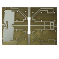
Rogers 3003 HDI Pcb , Rf Electronics Multilayer Printed Circuit Board 1.5mm Thickness
Key Specifications/Special Features:
Specification:
Board material: rogers 3003
Layer count: 4L
Board thickness: 1.5mm
Min hole size: 0.1mm
Min track width/space: 0.2mm/0.2mm
Copper thickness: 1oz
Solder mask: black/blue/green
Silkscreen: white
Surface finishing: Immersion Gold
Testing procedures for PCB board:
We perform multiple quality assuring procedures
before shipping out any PCB board. These include:
Visual Inspection
Flying probe
Impedance control
Solder ability detection
Digital metallogenic microscope
AOI (Automated Optical Inspection)
Quotation requirement:
Following specifications are needed for quotation:
Quantity
Base material
Board thickness
Copper thickness
Surface treatment
Color of solder mask and silkscreen
Shipping method and payment terms:
By DHL, UPS, FedEx, TNT using clients account.
DHL, UPS, FedEx, TNT forwarder of China.
We could ship the parcel by Russia Special Air Line for Russian
customer
(No tax in your there, 3 - 10 days to Moscow , 15-20 days to other
city)
By sea or air for mass quantity according to customer's
requirement.
By customer's Forwarder
Payment by PayPal, T/T, Western Union, and more.
Parameter:
o Item Data
1 Layer: 1 to 24 layers
2 Material type:FR-4, CEM-1, CEM-3, High TG, FR4 Halogen Free,
Rogers
3 Board thickness:0.20mm to 3.4mm
4 Copper thickness:0.5 OZ to 4 OZ
5 Copper thickness in hole:>25.0 um (>1mil)
6 Max. Board Size:(580mm×1200mm)
7 Min. Drilled Hole Size:4mil(0.1mm)
8 Min. Line Width:3mil (0.075mm)
9 Min. Line Spacing:3mil (0.075mm)
10 Surface finishing:HASL / HASL lead free, HAL, Chemical tin,
Chemical Gold, Immersion Silver/Gold, OSP, Gold plating
11 Solder Mask Color:Green/Yellow/Black/White/Red/Blue
12 Shape tolerance:±0.13
13 Hole tolerance:PTH: ±0.076 NPTH: ±0.05
14 Package:Inner packing: Vacuum packing / Plastic bag,Outer
packing: Standard carton packing
15 Certificate:UL,SGS,ISO 9001:2008
16 Special requirements:Buried and blind vias+controlled impedance
+BGA
17 Profiling:Punching, Routing, V-CUT, Beveling
Applications:
Amplifier Combiner Coupler Mixer Multiplexer Power divider WiFi
WiMAX, LTE bands 3G and 4G antenna
Typical Applications:
Parameter:
| o | Item | Data |
| 1 | Layer: | 1 to 24 layers |
| 2 | Material type: | FR-4, CEM-1, CEM-3, High TG, FR4 Halogen Free, Rogers |
| 3 | Board thickness: | 0.20mm to 3.4mm |
| 4 | Copper thickness: | 0.5 OZ to 4 OZ |
| 5 | Copper thickness in hole: | >25.0 um (>1mil) |
| 6 | Max. Board Size: | (580mm×1200mm) |
| 7 | Min. Drilled Hole Size: | 4mil(0.1mm) |
| 8 | Min. Line Width: | 3mil (0.075mm) |
| 9 | Min. Line Spacing: | 3mil (0.075mm) |
| 10 | Surface finishing: | HASL / HASL lead free, HAL, Chemical tin, Chemical Gold, Immersion Silver/Gold, OSP, Gold plating |
| 11 | Solder Mask Color: | Green/Yellow/Black/White/Red/Blue |
| 12 | Shape tolerance: | ±0.13 |
| 13 | Hole tolerance: | PTH: ±0.076 NPTH: ±0.05 |
| 14 | Package: | Inner packing: Vacuum packing / Plastic bag,Outer packing: Standard carton packing |
| 15 | Certificate: | UL,SGS,ISO 9001:2008 |
| 16 | Special requirements: | Buried and blind vias+controlled impedance +BGA |
| 17 | Profiling: | Punching, Routing, V-CUT, Beveling |
Karen-Sales Department
ShenZhen Xinchenger Electronics Co.,Ltd
sales3@xcepcb.com
Skype:karen-xcepcb


