

Active Member
|
[China]

Address: Headquarters :F12, Xingji Building Shangxing Road Shajing Town ,Baoan District Shenzhen China
Contact name:Rose Guo

Global Success Circuits Co.,Ltd |
|
|
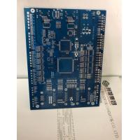
2OZ Copper Custom Printed Circuit Board 6 Layer PCB Medical 1.6MM thickness
Number of layers: 6 layers
Material: FR4
Board thickness: 1.6mm
Surface plating: Lead Free HASL
Special process description: 2OZ
Min Trace: 3mil
Brief introduction of GS:
1. GS are ISO/TS and UL certified.
2. We have 3 factories and more than 1000 employees in China.
3. With very compitive price and high quality, 50% pcb are exported to Europe and America.
GS can help your business stay ahead of the competition by improving quality, productivity, and delivery in your supply chain while reducing costs.
Welcome to send inquiry to me for comparing price any time.
PCBA/PCB assembly specifications:
What can we do for you?
For PCBA order, provide us:
Services and applications:
PCBA capabilities:
Competitive advantages:
| Item | Mass production | Small batch production | ||
| Number of layers | UP TO 18L | UP TO L | ||
| Laminate type | FR-4, halogen free, high TG(Shengyi, KB), Cem-3, PTFE, aluminum based, PTEE, Rogers or more. | FR-4, Halogen free, High TG(Shengyi, KB), Cem-3, PTFE, Aluminum based, PTEE, Rogers or more. | ||
| Maximum board size | 610mm*1100mm | 610mm*1100mm | ||
| Board thickness | 0.1mm-7.00mm | <0.1mm and >7.00mm | ||
| Minimum line width/space | 3.5mil(0.0875mm) | 3mil(0.075mm) | ||
| Minimum line gap | +/-15% | +/-10% | ||
| Outer layer copper thickness | 35um-175um | 35um-210um | ||
| Inner layer copper thickness | 12um-175um | 12um-210um | ||
| Drilling hole size(Mechanical) | 0.15mm-6.5mm | 0.15mm-6.5mm | ||
| Finished hole size (Mechanical) | 0.15mm-6.0mm | 0.15mm-6.0mm | ||
| Board thickness hole size ratio | 14:1 | 16:1 | ||
| Board thickness tolerance(t=0.8mm) | ±8% | ±5% | ||
| Board thickness tolerance(t<0.8mm) | ±10% | ±8% | ||
| Min. grid line width | 4mil(12, 18, 35um), 6mil(70um) | 4mil(12, 18, 35um), 6mil(70um) | ||
| Min. grid spacing | 6mil(12, 18, 35um), 8mil(70um) | 6mil(12, 18, 35um), 8mil(70um) | ||
| Hole size tolerance(Mechanical) | 0.05-0.075mm | 0.05mm | ||
| Hole position tolerance(Mechanical) | 0.005mm | 0.005mm | ||
| Solder mask color | Green, Blue, Black, White, Yellow, Red, Grey etc. | Green, Blue, Black, White, Yellow, Red, Grey etc. | ||
| Impedance control tolerance | +/-10% | +/-8% | ||
| Min. distance between drilling to conductor(non-blind buried orifice) | 8mil(8L), 9mil(10L), 10mil(14L), 12mil(26L) | 6mil(8L), 7mil(10L), 8mil(14L), 12mil(26L) | ||
| Min. Character width and height(35um base copper) | Line width: 5mil Height: 27mil | Line width: 5mil; height: 27mil | ||
| Max. test voltage | 500V | 500V | ||
| Max. test current | 200mA | 200mA | ||
Surface treatment | Flash Gold | 0.025-0.075um | 0.025-0.5um | |
| Immersion Gold | 0.05-0.1um | 0.1-0.2um | ||
| Sn/Pb HASL | 1-70um | 1-70um | ||
| Lead-free HASL | 1-70um | 1-70um | ||
| Immersion Silver | 0.08-0.3um | 0.08-0.3um | ||
| OSP | 0.2-0.4um | 0.2-0.4um | ||
| Gold Finger | 0.375um | >=1.75um | ||
| Hard Gold Plating | 0.375um | >=1.75um | ||
| Immersion Sin | 0.8um | |||
| V-Cut rest thickness tolerance | ±0.1mm | ±0.1mm | ||
Outline profile | Chamfer | The angle type of the chamfer | 30,45,60 | |
| Plug via hole | Max.size can be plugged | 0.6mm | ||
| Largest NPTH hole size | 6.5mm | >6.5mm | ||
| Largest PTH hole size | 6.5mm | >6.5mm | ||
| Min. solder spacer ring | 0.05mm | 0.05mm | ||
| Min. solder bridge width | 0.1mm | 0.1mm | ||
| Drilling diameter | 0.15mm-0.6mm | 0.15mm-0.6mm | ||
| Min. pad diameter with hole | 14mil( 0.15mm drilling) | 12mil( 0.1mm laser) | ||
| Min. BGA pad diameter | 10mil | 8mil | ||
| Chemical ENIG gold thickness | 0.025-0.1um(1-4U) | 0.025-0.1um | ||
| Chemical ENIG nickel thickness | 3-5um(120-200U) | 3-5um | ||
| Min. resistance test | Ω | 5 | ||


