

Active Member
|
[China]

Address: 3rd Building,Xinwuyuan Industrial Park, Difu Road,Gushu,Xixiang,Bao'an District,Shenzhen,China.
Contact name:PCB INQUIRY

Foisontech Corporation Co., Limited |
|
|
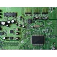
2 layer Electronic Pcb Board Components PCB Assembly & Pcba service Min. Line 0.12MM
1.Electronic components pcb assembling
2.Pcb with smt,smd,th-parts be soldered
3.Pcba test via AOI,X-ray
4.Build samples
Detailed Terms for Pcb Assembly
Technical requirement:
1) Professional Surface-mounting and Through-hole soldering
Technology
2) Various sizes like 1206,0805,0603 components SMT technology
3) ICT(In Circuit Test),FCT(Functional Circuit Test) technology.
4) PCB Assembly With UL,CE,FCC,Rohs Approval
5) Nitrogen gas reflow soldering technology for SMT.
6) High Standard SMT&Solder Assembly Line
7) High density interconnected board placement technology capacity.
Quote requirement:
1)Gerber file and Bom list
2)Clear pics of pcba or pcba sample for us
3)Test method for PCBA
One stop service for pcb design,pcb layout,pcb
manufacture,components purchasing,pcb assembly, test,packing and
pcb delivery.
PCB and PCBA specification
| 1 | layer | 1-18 layer | |
| 2 | Material | FR-4,CEM-1,CEM-3,Hight TG,FR4 Halogen Free,FR-1,FR-2 | |
| 3 | Board thickness | 0.2mm-4mm | |
| 4 | Max.finished board side | 800*508mm | |
| 5 | Min.drilled hole size | 0.25mm | |
| 6 | min.line width | 0.075mm(3mil) | |
| 7 | min.line spaceing | 0.075mm(3mil) | |
| 8 | Surface finish/treatment | HALS/HALS lead free,Chemical tin,Chemical Gold,Immersion gold Inmersion Silver/Gold,Osp,Gold Plating | |
| 9 | Copper thickness | 0.5-4.0oz | |
| 10 | Solder mask color | green/black/white/red/blue/yellow | |
| 11 | Inner packing | Vacuum packing,Plastic bag | |
| 12 | Outer packing | standard carton packing | |
| 13 | Hole tolerance | PTH:±0.076,NTPH:±0.05 | |
| 14 | Certificate | UL,ISO9001,ISO14001,ROHS,CQC | |
| 15 | profiling punching | Routing,V-CUT,Beveling | |
| 16. providing OEM service to all sorts of printed circuit board assembly | |||
| PRODUCTION CAPABILITY OF PCB | ||
PROCESS Engineer | ITEMS Item | PRODUCTION CAPABILITY Manufacturing Capability |
| Laminate | Type | FR-1,FR-5,FR-4 High-Tg,ROGERS,ISOLA,ITEQ, ALUMINUM,CEM-1,CEM-3,TACONIC,ARLON,TEFLON |
| Thickness | 0.2~3.2mm | |
| Production Type | Layer Count | 2L-16L |
| Surface Treatment | HAL,Gold Plating,Immersion Gold,OSP, Immersion Silver,Immersion Tin,Lead Free HAL | |
| Cut Lamination | Max. Working Panel size | 1000×1200mm |
| Inner Layer | Internal Core Thickness | 0.1~2.0mm |
| Internal width/spacing | Min: 4/4mil | |
| Internal Copper Thickness | 1.0~3.0oz | |
| Dimension | Board Thickness Tolerance | ±10% |
| Interlayer Alignment | ±3mil | |
| Drilling | Manufacture Panel Size | Max: 650×560mm |
| Drilling Diameter | ≧0.25mm | |
| Hole Diameter Tolerance | ±0.05mm | |
| Hole Position Tolerance | ±0.076mm | |
| Min.Annular Ring | 0.05mm | |
| PTH+Panel Plating | Hole Wall copper Thickness | ≧20um |
| Uniformity | ≧90% | |
| Outer Layer | Track Width | Min: 0.08mm |
| Track Spacing | Min: 0.08mm | |
| Pattern Plating | Finished Copper Thickness | 1oz~3oz |
| EING/Flash Gold | Nickel Thickness | 2.5um~5.0um |
| Gold Thickness | 0.03~0.05um | |
| Solder Mask | Thickness | 15~35um |
| Solder Mask Bridge | 3mil | |
| Legend | Line width/Line spacing | 6/6mil |
| Gold Finger | Nickel Thickness | ≧120u〞 |
| Gold Thickness | 1~50u〞 | |
| Hot Air Level | Tin Thickness | 100~300u〞 |
| Routing | Tolerance of Dimension | ±0.1mm |
| Slot Size | Min:0.4mm | |
| Cutter Diameter | 0.8~2.4mm | |
| Punching | Outline Tolerance | ±0.1mm |
| Slot Size | Min:0.5mm | |
| V-CUT | V-CUT Dimension | Min:60mm |
| Angle | 15°30°45° | |
| Remain Thickness Tolerance | ±0.1mm | |
| Beveling | Beveling Dimension | 30~300mm |
| Test | Testing Voltage | 250V |
| Max.Dimension | 540×400mm | |
| Impedance Control | Tolerance | ±10% |
| Aspect Ration | 12:1 | |
| Laser Drilling Size | 4mil(0.1mm) | |
| Special Requirements | Buried And Blind Via, Impedance Control, Via Plug, BGA Soldering and Gold Finger Are Acceptable | |
| OEM&ODM Service | Yes | |
How to get quick quotation?
![]()
| Step 1 Please send us Gerber file with these format: .CAD / .Gerber / .PCB / .DXP / .P-CAD, etc | ||||||||||||||||||||
| Step 2 Also please provide us the below details for quick quotation: | ||||||||||||||||||||
Board material: Fr - 4 / CEM - 1 / CEM - 3 / 22F / Fr - 1 / others | ||||||||||||||||||||
| Material brand: SY / KB / Rogers (optional) | ||||||||||||||||||||
| Material Specification:High Tg / copper based / aluminum based or others (optional) | ||||||||||||||||||||
| Board thickness: 0.1 - 6.0 mm | ||||||||||||||||||||
| Copper thickness: 0.05 Oz - 8 Oz ( 17 um - 288 um ) | ||||||||||||||||||||
| Surface Treatment: OSP / ENIG / HASL / Lead Free HASL / Immersion Tin / Immersion Sin | ||||||||||||||||||||
| Color of solder mask and silk print: Green / red / blue / black / white / yellow ,etc | ||||||||||||||||||||
| Board size and quantity | ||||||||||||||||||||
If you don't have Gerber file, please provide us the imfomation as step 2 or post your PCB Board to us for clone.
| ||||||||||||||||||||
SAMPLE:
| ||||||||||||||||||||
| ||||||||||||||||||||
| Layer count | Sample lead time/workday | Batch lead time/workday |
| 1-2L | 2 | 6 |
| 4L | 5 | 8 |
| 6L | 5 | 9 |
| 8L | 6 | 10 |
| 10L | 8 | 10 |
| 12L | 8 | 12 |
| 14L | 10 | 15 |
| 16L | 10 | 18 |
| 18-40L (Up to difficulty) | at least 18 | at least 24 |
| P.S. For HDI, Blind/Buried Hole PCB: Regular Lead Time + 3 workdays | ||
Q1: I am used to designing in metric units while the website is specified in imperial units.
A: When requesting an online quote, the quote form can handle mm units as well as inches for dimensions.
Q2: How do I specify internal cutouts/milling in my design?
A: All internal cutouts/slots/milling should be specified on the same layer is the board outline. The the minimum routable slot size is 32 mils. During order time, please state this requirement in the "Special Request" section so that our CAM engineers is aware of it. This is not something we encounter.
Q3: What are the available holes sizes?
A: 14 mils to 150 mils - 1 mil increments 150 mils to 200 mils - 5 mil increments above 200 mils - holes would be routed out We only use drills in imperial units. Files submitted in metric units (mm) would be converted to imperial units (mils) and rounded up to the next mil.
Now send us your inquiry, and you will be replied within 8 hours!
Little knowledge - Consideration about PCB fabrication
When placed an order of PCBs (printed circuit boards), you should
spend time to considerate the basic factors including PCB board
substrate material, layer count, board size, board thickness,
copper thickness, surface finish, solder mask, silkscreen, blind
vias, buried vias, through-hole plating, SMT and so on. When all
the factors are checked and confirmed with the engineers, we highly
recommended sample tested before the real fabrication of your PCB
boards. If all things go well, fabrication could be started right
away. However, it may need to do some modification if customer is
not satisfied with the sample.


