

Active Member
|
[China]

Address: Ailian Lian'ai Building, Longgang District, Shenzhen
Contact name:Xue Wang

Shenzhen Chuangying Times Technology Co., Ltd. |
|
|
This is the leftover material after Jin Yuan is cut, and the wafer
can also be taken out. Each chip can take about 130 wafers, and the
box is sent by air in a box of three kilograms. It can also be
shipped in domestic ports. If necessary, please contact us. Taiwan
channel direct hair.
This is a subsidiary of our group for wafer and chip projects (uncut material, defective brand, finished product), and usable wafers can be removed for uncut material and defective products. Market uses are as follows:
5nm wafer 5NANO technology wafer component chip applications cover:
| 5nm wafer 5NANO technology wafer component chip applications cover: |
| ❶ Smartphone. |
| ❷AI machine system high-speed operation. |
| ❸Connect with high-end multi-party platforms such as the Internet of Things and smart cities. |
| ❹Logical calculation analysis and judgment (safety automotive IC). |
| ❺NANDR Flash random access device. Flash memory (pen drive DRAM). |
| ❻ Analog IC. Sensor. |
| ❼Microcontroller; laser cell protein medical beauty precision instrument. |
A large number of 5NANO 12” wafer processes use EUV (Extreme Ultraviolet Photolithography) technology that will continue to improve EUV’s production efficiency and yield technology. All three can be used in common.
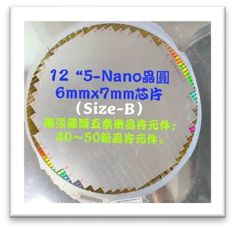
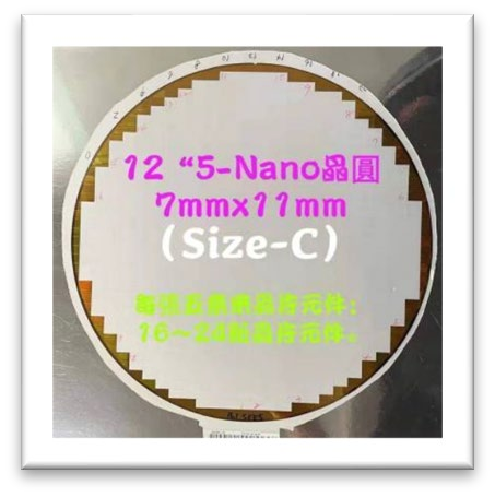
㊀ The 12-inch 5nm chip is available in three sizes:
①.4*6m/m, ②.6*7m/m, ③.7*11m/m.
㊁The lithography line is made:
①.4*6mm is an area of 24 square millimeters, and each square millimeter has more than 177 million transistors implanted, that is, about 4.248 billion transistors, and the conversion access memory = 512MB capacity.
②.6*7mm, with a total of 7.434 billion transistors, equivalent to 1GB capacity.
③.7*11mm, there are 13.629 billion transistors in total, which is equivalent to 1.5G capacity.
Quantity: A total of 1000 boxes per month can be ordered (1.2 million pieces) / minimum order of 40 boxes (9600 pieces),
Try a box of 240 pieces. (Sample price USD 7 / PCS).
Supply period: long orders can be signed and delivered in batches
Product Specifications:
Several key points of wafer tailing processing are explained:
Global standard 12”5Nano wafer wafer, the outer periphery of each film is approximately
Size- A 4mm * 6mm.(About 70 to 110 chips) Size- B 6mm * 7mm.(About
40 to 50 chips) Size- C 7mm * 11mm.(About 16 to 24 chips)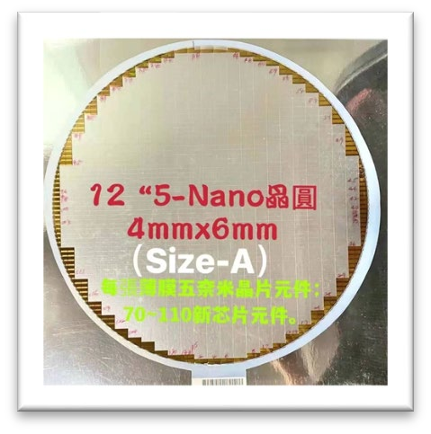
Packaged form: Including SoIC (system integrated chip), InFO (integrated fan-out packaging technology),
3DIC technology platforms such as CoWoS (Chip on Substrate Packaging), these 5nm chips are all suitable for fan in or fanout type advanced packaging technology. Although QFN, SOP, LQF, and these are all too low-end, they can all be packaged. If a lower-end packaging technology is used, it depends on the matching with the carrier board.
Package:
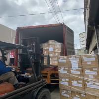
Carton packaging. 1kg is 80 pieces.
By air it is 3kg per box (240 pieces) By sea it is 15kg per box (1200 pieces)
The container is 1000 boxes (1.2 million pieces) 15 tons in weight
Five-nanometer wafer sample testing identifies detailed data descriptions:
The level of packaging technology requires a "five-nanometer chip" packaging factory to detect, and the packaging results are necessary and necessary to apply high-tech righteousness. "Optoelectronics Technology Professional Instrument" can detect more than 1....7E per cubic millimeter. "Transistor Structure" This instrument has 3D comprehensive functions.
Provide test data in Taiwan: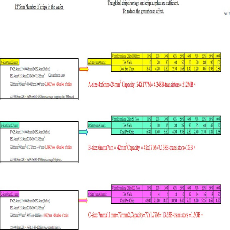
Excerpted from the Internet, for reference only
Finally, if you have any questions you want to know, please leave a
message in the comment area!
(Disclaimer: The above content comes from the fund bar, which only
represents the personal views of the netizens of the fund bar, and
has nothing to do with the daily fund platform. The rate of return
data is for reference only, past performance does not indicate
future performance, nor does it constitute investment advice.
Investors Take your own risk. There are risks in the market and
investment needs to be cautious.
Judging from the news from the production side, chip manufacturers
have not been affected too much for the time being. On May 13, Wu
Jincheng, director of the Shanghai Municipal Commission of Economy
and Information Technology, introduced at the press conference that
in the field of integrated circuits, chip manufacturing companies
have maintained more than 90% of their production capacity. A
number of equipment, materials, packaging and testing and other
supporting enterprises in the industrial chain have accelerated
their resumption of work.


