Active Member
|
[China]

Address: 6-11C Shidai Jingyuan Fuyong Town, Baoan District, Shenzhen City, Guangdong Province, China
Contact name:Sally Mao

Shenzhen Bicheng Electronics Technology Co., Ltd |
|
|
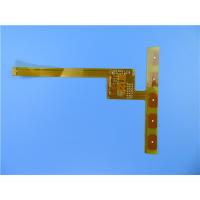
Dual Layer Flexible PCB Built on Polyimide With Immersion Gold and Yellow Mask
(FPC’s are custom-made products, the picture and parameters shown are just for reference)
General description
This is a type of flexible printed circuit for the application of analog device. It’s a 2 layer board at 0.15mm thick. The base laminate is from ITEQ, It's fabricated per IPC 6012 Class 2 using supplied Gerber data. Immersion gold is applied on the pads. Stiffener is applied on the connector part.
Parameter and data sheet
| Number of Layers | 2 |
| Board Type | Flexbile cirucit |
| Board Thickness | 0.15mm +/-10% |
| Board Material | Polyimide (PI) 25um |
| Board Material Supplier | ITEQ |
| Tg Value of Board Material | 60℃ |
| PTH Cu thickness | ≥20 um |
| Inner Iayer Cu thicknes | N/A |
| Surface Cu thickness | 35 um (1oz) |
| Coverlay Colour | Yellow |
| Number of Coverlay | 2 |
| Thickness of Coverlay | 25 um |
| Stiffener | 200 um |
| Type of Silkscreen Ink | IJR-4000 MW300 |
| Supplier of Silkscreen | TAIYO |
| Color of Silkscreen | White |
| Number of Silkscreen | 2 |
| Mininum Trace (mil) | 4 mil |
| Minimum Gap(mil) | 4 mil |
| Surface Finish | Immersion Gold |
| RoHS Required | Yes |
| Famability | 94-V0 |
| Thermal Shock Test | Pass, -25℃±125℃, 1000 cycles. |
| Thermal Stress | Pass, 300±5℃,10 seconds, 3 cycles. No delamination, no blistering. |
| Function | 100% Pass electrical test |
| Workmanship | Compliance with IPC-A-600H & IPC-6013C Class 2 |

Features and benefits
Excellent flexibility
Reducing the volume
Weight reduction
Consistency of assembly
Increased reliability
Controllability of electrical parameter design
The end can be whole soldered
Low cost
Continuity of processing
Focus on low to medium volume production
Applications
Thin-film switch, mobile phone antenna flex board, automobile GPS navigation flex board
Structure of Flexible PCB
According to the number of layers of conductive copper foil, FPC can be divided into single layer circuit, double layer circuit, multi-layer circuit, double sided and so on.
Single-layer structure: the flexible circuit of this structure is the simplest structure of the flexible PCB. Usually the base material (dielectric substrates) + transparent rubber(adhesive) + copper foil is a set of purchased raw materials(semi-manufactures), the protective film and transparent glue are another kind of bought raw material. First, copper foil must be etched to obtain the required circuit, and the protective film should be drilled to reveal the corresponding pad. After cleaning, the two are combined by rolling. Then the exposed part of the pad electroplated gold or tin to protect. In this way, the big panel board will be ready. Generally also it’s stamped into the corresponding shape of the small circuit board. There is also no protective film directly on the copper foil, but printed resistance soldering coating, so that the cost will be lower, but the mechanical strength of the circuit board will become worse. Unless the strength requirement is not high and the price needs to be as low as possible, it is best to apply the protective film method.
Double layer structure: when the circuit is too complex to be wired, or copper foil is needed to shield the ground, it is necessary to choose a double layer or even a multilayer. The most typical difference between a multilayer and a single plate is the addition of a perforated structure to connect the layers of copper foil. The first process of transparent rubber + base material + copper foil is to make holes. Drill holes in the base material and copper foil first, clean and then plated with a certain thickness of copper. The subsequent fabrication process is almost the same as the single-layer circuit.
Double sided structure: both sides of the double sided FPC have pads, mainly used to connect other circuit boards. Although it and monolayer structure is similar, but the manufacturing process is very different. Its raw material is copper foil, protective film and transparent glue. The protective film should be drilled according to the position of the pad first, then the copper foil should be affixed, the pad and track lines should be etched and then the protective film of another drilled hole should be affixed.