

Active Member
|
[China]

Address: 6-11C Shidai Jingyuan Fuyong Town, Baoan District, Shenzhen City, Guangdong Province, China
Contact name:Sally Mao

Shenzhen Bicheng Electronics Technology Co., Ltd |

|
|
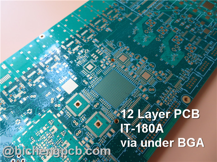
Why do we need to use via in PCB? And its Parasitic Capacitance and Parasitic Inductance
Tag# PCB design, Multi-layer PCB, High density interconnection PCB
PCB holes
Via is one of the important parts of multi-layer PCB, and the cost of drilling usually accounts for 30% to 40% of the cost of PCB fabrication. Briefly, every hole in the PCB can be called a via. From the point of view of function, the hole
can be divided into two categories: one is used as the electrical connection between the layers, the other is used as the fixing or positioning of the device. These holes are generally divided into three types, namely blind hole (blind via), buried hole (buried via) and through hole (through via).
1.1 Composition of Holes
The blind hole is located on the top and bottom surface of the printed circuit board and has a certain depth for the connection between the surface line and the inner line below. The depth of the hole usually does not exceed a certain ratio (aperture). Buried hole is a connecting hole located in the inner layer of the printed circuit board, which does not extend to the surface of the circuit board.
The above two kinds of holes are located in the inner layer of the circuit board. The formation of through hole process is used before lamination, and several inner layers may be overlapped done during the formation of the through hole.
The third is called a through hole, which passes through the entire circuit board. It can be used to interconnect internally or as an installation location hole for components. Because the through hole is easier to realize and the cost is low, it is used in most printed circuit boards instead of the other two. The following mentioned holes, without special instructions, are considered as through holes.
From the design point of view, a hole is mainly composed of two parts, one is the middle hole (drill hole), the other is the pad area around the hole, see below. The size of these two parts determines the size of the hole. Clearly, in
high-speed, high-density PCB design, designers always want the holes the smaller the better, so that it can leave more wiring space on the board.

In addition, the smaller the hole, the lower its own parasitic capacitance, and more suitable for high-speed circuits. The reduction of the hole size brings about the increase of the cost, and the size of the hole can not be reduced without restriction. It is limited by the technology of drilling and electroplating and so on.
The smaller the hole, the longer it takes to drill the hole, and the easier it is to deviate from the center position; and when the depth of the hole exceeds 6 times the diameter of the hole, it can not be guaranteed that the hole wall can be uniformly copper plated. Now, for example, the normal thickness of a PCB (depth of through hole) is 1.6mm, so the minimum diameter of the hole provided by the PCB manufacturer can only reach 0.2mm.
1.2 Parasitic Capacitance of Vias
The via itself has parasitic capacitance to the ground. Where it is known that the diameter of the isolating hole on the ground layer is D2, the diameter of the via pad is D1, the thickness of the PCB is T, the dielectric constant of the substrate is ε, then the vale of the parasitic capacitance through the hole is approximately as follows:
C=1.41εTD1/(D2-D1).

The main effect of the parasitic capacitance through the hole is to prolong the rising time of the signal and reduce the speed of the circuit. For example, a PCB board with 50 mil thick, if you use a via with 10mil inner diameter and 20 mil pad diameter, 32 mil distance between pad and ground copper area, then we can approximately get the parasitic capacitance of the via by the above formula: C=1.41 x4.4x0.050x0.020/(0.032-0.020)=0.517pF. The variable quantity of this part of the capacitance caused by the rising time is: T10-90=2.2 C (Z0/2)=2.2 x0.517x(55/2)=31.28 ps.
From these values, it can be seen that although the utility of the rising delay caused by the parasitic capacitance of a single via is not obvious, the designer should take it into consideration that if the multiple vias are used between layers.

1.3 Parasitic Inductance of Vias
Besides parasitic capacitance, there is parasitic inductance at the same time through vias. In the design of high speed digital circuit, the harm caused by the parasitic inductance through the hole is often greater than that of the parasitic capacitance. Its parasitic series inductance weakens the contribution of bypass capacitance and weakens the filtering utility of the whole power supply system. We can use the following formula to simply calculate an approximate parasitic inductance of the via:
L=5.08h[ln(4h/d) +1].

Where L refers to the inductance of the via, h the length of the via, d the diameter of the via. It can be seen from the formula that the diameter of the via has little effect on the inductance, but the biggest effect on the inductance is the length of the via. Still using the above example, it can be calculated that the inductance of the via is: L=5.08 x0.050[ln (4x0.050/0.010)1]=1.015 nH. When the rising time of the signal is 1 ns, the equivalent impedance is: XL=πL/T10-90=3.19Ω. Such impedance can not be ignored in the passage of high frequency current. In particular, the bypass capacitance needs to pass through two vias when connecting the power layer and the ground layer, so that the parasitic inductance of the vias will increase exponentially.

1.4 Design of via in High Speed PCB
From the above analysis of the parasitic characteristics of the vias, we can see that in the design of high speed PCB, the seemingly simple via often brings great negative effects to the design of the circuit. In order to reduce the adverse effect of the parasitic effect from the via, we can try to do it in the design as follows:
1) Considering the cost and signal quality, choose a reasonable size for the vas. Such as 6-10 layer memory module PCB design,10/20 mil (drilling / pad) via is better; for some high density small size board, you can also try to use 8/18 mil via. At present, since the laser drilling machines are used in the fabrication, it is possible to use smaller size holes under technical conditions. For the via of the power supply or ground wire, a larger size can be considered
to reduce the impedance.
| Printed Circuit Board Capability 2020 | |
| Parameter | Value |
| Layer Counts | 1-32 |
| Substrate Material | FR-4(including High Tg 170, High CTI>600V); Aluminum based; Copper based; Rogers RO4350B, RO4003C, RO3003, RO3006, RO3010, RO3210 etc.; Rogers RT/duroid 5880, RT/duroid 5870, RT/duroid 6002, RT/duroid 6010 etc..; Taconic TLX-8, TLY-5, RF-35TC, TLF-35 etc..; Arlon AD450, AD600 etc; PTFE F4B DK2.2, DK2.65 etc..; Polyimide and PET. |
| Maximum Size | Flying test: 900*600mm, Fixture test 460*380mm, No test 1100*600mm |
| Board Outline Tolerance | ±0.0059" (0.15mm) |
| PCB Thickness | 0.0157" - 0.3937" (0.40mm--10.00mm) |
| Thickness Tolerance(T≥0.8mm) | ±8% |
| Thickness Tolerance(t<0.8mm) | ±10% |
| Insulation Layer Thickness | 0.00295" - 0.1969" (0.075mm--5.00mm) |
| Minimum Track | 0.003" (0.075mm) |
| Minimum Space | 0.003" (0.075mm) |
| Outer Copper Thickness | 35µm--420µm (1oz-12oz) |
| Inner Copper Thickness | 17µm--420µm (0.5oz - 12oz) |
| Drill Hole(Mechanical) | 0.0059" - 0.25" (0.15mm--6.35mm) |
| Finished Hole(Mechanical) | 0.0039"-0.248" (0.10mm--6.30mm) |
| DiameterTolerance(Mechanical) | 0.00295" (0.075mm) |
| Registration (Mechanical) | 0.00197" (0.05mm) |
| Aspect Ratio | 12:1 |
| Solder Mask Type | LPI |
| Min Soldermask Bridge | 0.00315" (0.08mm) |
| Min Soldermask Clearance | 0.00197" (0.05mm) |
| Plug via Diameter | 0.0098" - 0.0236" (0.25mm--0.60mm) |
| Impedance Control Tolerance | ±10% |
| Surface Finish | HASL,HASL LF,ENIG,Imm Tin,Imm Ag, OSP, Gold Finger |


