Active Member
|
[China]

Address: Room 36B1-B2, Building C, Electronics Science & Technology Building Shennan Mid-Road, Shenzhen China
Contact name:Sharon Yang

Anterwell Technology Ltd. |

|
|
Stock Offer (Hot Sell)
| Part No. | Quantity | Brand | D/C | Package |
| IS63LV1024L-10TLI | 5170 | ISSI | 15+ | TSOP |
| IS66WVE4M16BLL-70BLI | 3926 | ISSI | 12+ | BGA |
| ISD2590PY | 2942 | ISD | 15+ | DIP |
| ISL12022IBZ | 1981 | INTERSIL | 16+ | SOP-8 |
| ISL21080CIH315Z-TK | 4977 | INTERSIL | 15+ | SOT-23 |
| ISL54405IRUZ-T | 6430 | INTERSIL | 13+ | QFN16 |
| ISL55016IRTZ | 4989 | INTERSIL | 16+ | FDAN-6 |
| ISL6227HRZ | 2675 | INTERSIL | 14+ | QFN |
| ISL62281HRTZ-T | 2717 | INTERSIL | 11+ | QFN |
| ISL6264CRZ | 7698 | INTERSIL | 16+ | QFN |
| ISL6265CHRTZ-T | 9438 | INFERSIL | 12+ | TQFN48 |
| ISL6267HRZ-T | 10967 | INTERSIL | 16+ | QFN |
| ISL62870HRUZ-T | 2746 | INTERSIL | 10+ | QFN |
| ISL62882HRTZ | 8082 | INTERSIL | 12+ | QFN40 |
| ISL6291-2CRZ | 9822 | INTERSIL | 16+ | QFN |
| ISL9492ERZ-T | 2817 | INTERSIL | 11+ | QFN |
| ISL95831HRTZ | 2888 | INTERSIL | 16+ | QFN48 |
| ISL9V3040D3ST | 9593 | FAIRCHILD | 14+ | TO-252 |
| ISO1H811G | 5966 | 14+ | SSOP-36 | |
| ISO3082DWR | 5257 | TI | 16+ | SOP-16 |
| ISO7240MDWR | 4571 | TI | 16+ | SOP-16 |
| ISPLSI2032A-80LJ44 | 3353 | LATTICE | 05+ | PLCC |
| IT8512E-JXA | 932 | ITE | 08+ | TQFP128 |
| ITR8307/F43 | 16473 | EVERLIGHT | 14+ | DIP-4 |
| ITS4880R | 1090 | 14+ | HSSOP36 | |
| IXFH26N50 | 1930 | IXYS | 12+ | TO-247 |
| IXFK44N50 | 3503 | IXYS | 01+ | TO-264 |
| IXFN48N50Q | 2332 | IXYS | 16+ | SOT-227 |
| IXGR48N60C3D1 | 5060 | IXYS | 13+ | TO-247 |
| J111 | 15000 | FSC | 16+ | TO-92 |
PROCESSOR SUPERVISORY CIRCUITS
features
applications
description
The TPS382x family of supervisors provides circuit initialization and timing supervision, primarily for DSP and processor-based systems.
During power-on, RESET is asserted when supply voltage VDD becomes higher than 1.1 V. Thereafter, the supply voltage supervisor monitors VDD and keeps RESET active as long as VDD remains below the threshold voltage VIT–.
An internal timer delays the return of the output to the inactive state (high) to ensure proper system reset. The delay time, td, starts after VDD has risen above the threshold voltage VIT–. When the supply voltage drops below the threshold voltage VIT–, the output becomes active (low) again. N
o external components are required. All the devices of this family have a fixed-sense threshold voltage VIT– set by an internal voltage divider.
The TPS3820/3/5/8 devices incorporate a manual reset input, MR. A low level at MR causes RESET to become active. The TPS3824/5 devices include a high-level output RESET. TPS3820/3/4/8 have a watchdog timer that is periodically triggered by a positive or negative transition at WDI.
When the supervising system fails to retrigger the watchdog circuit within the time-out interval, ttout, RESET becomes active for the time period td. This event also reinitializes the watchdog timer. Leaving WDI unconnected disables the watchdog.
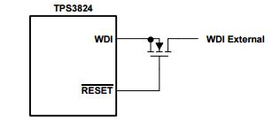
In applications where the input to the WDI pin may be active (transitioning high and low) when the TPS3820/3/4/8 is asserting RESET, the TPS3820/3/4/8 does not return to a non-reset state when the input voltage is above Vt.
If the application requires that input to WDI is active when RESET is asserted, WDI must be decoupled from the active signal. This can be accomplished by using an N-channel FET in series with the WDI pin, with the gate of the FET connected to the RESET output as shown in Figure 1.
Figure 1
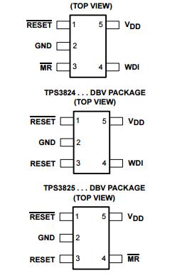
The product spectrum is designed for supply voltages of 2.5 V, 3 V, 3.3 V, and 5 V. The circuits are available in a 5-pin SOT23-5 package. The TPS382x devices are characterized for operation over a temperature range of -40°C to 85°C.
absolute maximum ratings over operating free-air temperature range
(unless otherwise noted)†
Supply voltage, VDD (see Note 1) . . . . . . . . . . . . . . . . . . . . . . . . . . . . . . . . . . . . . . . . . . . . . 6 V
RESET, RESET, MR, WDI (see Note 1) . . . . . . . . . . . . . . . . . . . . . . . . . . –0.3 V to (VDD + 0.3 V)
Maximum low output current, IOL . . . . . . . . . . . . . . . . . . . . . . . . . . . . . . . . . . . . . . . . . . . . . . 5 mA
Maximum high output current, IOH . . . . . . . . . . . . . . . . . . . . . . . . . . . . . . . . . . . . . . . . . . . . . –5 mA
Input clamp current range, IIK (VI < 0 or VI > VDD) . . . . . . . . . . . . . . . . . . . . . . . . . . . . . . . . ±10 mA
Output clamp current range, IOK (VO < 0 or VO > VDD) . . . . . . . . . . . . . . . . . . . . . . . . . . . . . ±10 mA
Continuous total power dissipation . . . . . . . . . . . . . . . . . . . . . . . . . . . . See Dissipation Rating Table
Operating free-air temperature range, TA . . . . . . . . . . . . . . . . . . . . . . . . . . . . . . . . . . –40°C to 85°C
Storage temperature range, Tstg . . . . . . . . . . . . . . . . . . . . . . . . . . . . . . . . . . . . . . . . –65°C to 150°C
Soldering temperature . . . . . . . . . . . . . . . . . . . . . . . . . . . . . . . . . . . . . . . . . . . . . . . . . . . . . . . . 260°C
Stresses beyond those listed under “absolute maximum ratings” may cause permanent damage to the device. These are stress ratings only, and functional operation of the device at these or any other conditions beyond those indicated under “recommended operating conditions” is not implied. Exposure to absolute-maximum-rated conditions for extended periods may affect device reliability.
NOTE 1: All voltage values are with respect to GND.
TPS3820, TPS3823, TPS3828 . . . DBV PACKAGE
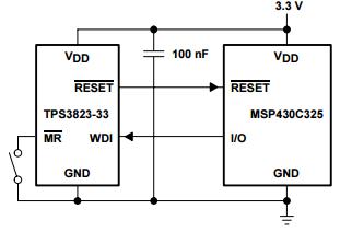
typical application