

Active Member
|
[China]

Address: Room 36B1-B2, Building C, Electronics Science & Technology Building Shennan Mid-Road, Shenzhen China
Contact name:Sharon Yang

Anterwell Technology Ltd. |

|
|
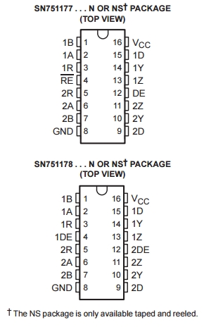
SN751177, SN751178
DUAL DIFFERENTIAL DRIVERS AND RECEIVERS
• Meet or Exceed the Requirements of ANSI Standards TIA/EIA-422-B and TIA/EIA-485-A and ITU Recommendations V.10 and V.11
• Designed for Multipoint Bus Transmission on Long Bus Lines in Noise Environments
• Driver Positive- and Negative-Current Limiting
• Thermal Shutdown Protection
• Driver 3-State Outputs
• Receiver Common-Mode Input Voltage Range of –12 V to 12 V
• Receiver Input Sensitivity... ±200 mV
• Receiver Hysteresis . . . 50 mV Typ
• Receiver Input Impedance . . . 12 kΩ Min
• Receiver 3-State Outputs (SN751177 Only)
• Operate From Single 5-V Supply
description
The SN751177 and SN751178 dual differential drivers and receivers are monolithic integrated circuits that are designed for balanced multipoint bus transmission at rates up to 10 Mbit/s. They are designed to improve the performance of full-duplex data communications over long bus lines and meet ANSI Standards TIA/EIA-422-B and TIA/EIA-485-A and ITU Recommendations V.10 and V.11.
The SN751177 and SN751178 driver outputs provide limiting for both positive and negative currents and thermal-shutdown protection from line-fault conditions on the transmission bus line.
The receiver features high input impedance of at least 12 kΩ, an input sensitivity of ±200 mV over a common-mode input voltage range of –12 V to 12 V, and typical input hysteresis of 50 mV. Fail-safe design ensures that if the receiver inputs are open, the receiver outputs always will be high.
The SN751177 and SN751178 are characterized for operation from –20°C to 85°C.
absolute maximum ratings over operating free-air temperature range
(unless otherwise noted)†
Supply voltage, VCC (see Note 1) . . . . . . . . . . . . . . . . . . . . . . . . . . . . . . . . . . . . . . . . . . . .7 V
Input voltage, VI (DE, RE, and D inputs) . . . . . . . . . . . . . . . . . . . . . . . . . . . . . . . . . . . . . . . 7 V
Receiver input voltage range, VI (A or B inputs) . . . . . . . . . . . . . . . . . . . . . . . . . –25 V to 25 V
Receiver differential input voltage range, VID (see Note 2) . . . . . . . . . . . . . . . . . –25 V to 25 V
Driver output voltage range, VO . . . . . . . . . . . . . . . . . . . . . . . . . . . . . . . . . . . . . –10 V to 15 V
Receiver low-level output current, IOL . . . . . . . . . . . . . . . . . . . . . . . . . . . . . . . . . . . . . . . 50 mA
Package thermal impedance, θJA (see Note 3): N package . . . . . . . . . . . . . . . . . . . . . . 78°C/W
NS package . . . . . . . . . . . . . . . . . . . . . 111°C/W
Storage temperature range, Tstg . . . . . . . . . . . . . . . . . . . . . . . . . . . . . . . . . . . . –65°C to 150°C
Lead temperature 1,6 mm (1/16 inch) from case for 10 seconds . . . . . . . . . . . . . . . . . . . . 260°C
† Stresses beyond those listed under “absolute maximum ratings” may cause permanent damage to the device. These are stress ratings only, and functional operation of the device at these or any other conditions beyond those indicated under “recommended operating conditions” is not implied. Exposure to absolute-maximum-rated conditions for extended periods may affect device reliability.
NOTES:
1. All voltage values, except differential input voltage, are with respect to the network ground terminal.
2. Differential input voltage is measured at the noninverting terminal with respect to the inverting terminal.
3. The package thermal impedance is calculated in accordance with JESD 51, except for through-hole packages, which use a trace length of zero.
Stock Offer (Hot Sell)
| Part no. | Quantity | Brand | D/C | Package |
| CNY65 | 800 | VISHAY | 15+ | DIP |
| DAC5571IDB | 800 | TI | 16+ | SOT23 |
| KMT32 | 800 | MEASUREM | 16+ | SOP8 |
| L6386D | 800 | ST | 14+ | SOP14 |
| RTL8201BL-LF | 800 | REALTEK | 14+ | QFP |
| TOP209PN | 800 | POWER | 14+ | DIP-8 |
| TPS5430DDA | 800 | TI | 16+ | SOP-8 |
| OPA2544T | 811 | TI | 16+ | TO220-11 |
| SA571D | 811 | ON | 13+ | SOP-16 |
| W24258S-70LL | 812 | WINBOND | 15+ | SOP28 |
| FSDM0465R | 820 | FSC | 16+ | TO-220-6F |
| LM2696MXA | 820 | NS | 16+ | TSSOP |
| SM8S30AHE3/2D | 820 | VISHAY | 14+ | DO-218AB |
| MIP2H2 | 830 | PANASONIC | 14+ | DIP-7 |
| 88E1322-LKJ | 841 | MARVELL | 14+ | QFP |
| BCY79 | 845 | ST | 16+ | TO-18 |
| IRF4905S | 870 | IR | 16+ | TO-263 |
| HC541 | 875 | TI | 13+ | SOP20 |
| HCS200/SN | 875 | MICROCHIP | 15+ | SOP8 |
| ADP3338AKC-5.0 | 880 | AD | 16+ | SOT-223 |
| IRFB31N20D | 882 | IR | 16+ | TO-220 |
| L9113 | 885 | ST | 14+ | QFP |
| 2SC2553 | 887 | TOSHIBA | 14+ | TO-220 |
| MX29LV320BTC-70 | 887 | MXIC | 14+ | SOP |
| A3953SLB | 888 | ALLEGRO | 16+ | SOP |
| CD74HC4067M96 | 888 | TI | 16+ | SOP |
| K9F1G08UOB-PCBO | 888 | SAMSUNG | 13+ | TSOP48 |
| M51957BL | 888 | RENESAS | 15+ | SIP-5 |
| STM8309T | 888 | SAMHOP | 16+ | SOP8 |
| VB025 | 888 | ST | 16+ | SOP10 |


