

Active Member
|
[China]

Address: Room 36B1-B2, Building C, Electronics Science & Technology Building Shennan Mid-Road, Shenzhen China
Contact name:Sharon Yang

Anterwell Technology Ltd. |

|
|
UCC2808A-1, UCC2808A-2, UCC3808A-1, UCC3808A-2
LOW POWER CURRENT MODE PUSH-PULL PWM
• Dual Output Drive Stages in Push-Pull Configuration
• Current Sense Discharge Transistor to Improve Dynamic Response
• 130-µA Typical Starting Current
• 1-mA Typical Run Current
• Operation to 1 MHz
• Internal Soft Start
• On-Chip Error Amplifier With 2-MHz Gain Bandwidth Product
• On Chip VDD Clamping
• Output Drive Stages Capable of 500-mA Peak-Source Current, 1-A Peak-Sink Current
description
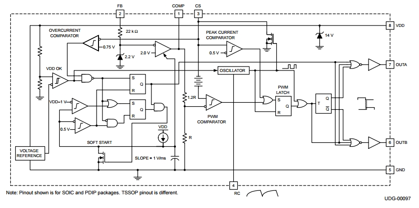
The UCC3808A is a family of BiCMOS push-pull, high-speed, low-power, pulse-width modulators. The UCC3808A contains all of the control and drive circuitry required for off-line or dc-to-dc fixed frequency current-mode switching power supplies with minimal external parts count.
The UCC3808A dual output drive stages are arranged in a push-pull configuration. Both outputs switch at half the oscillator frequency using a toggle flip-flop. The dead time between the two outputs is typically 60 ns to 200 ns depending on the values of the timing capacitor and resistors, thus limiting each output stage duty cycle to less than 50%.
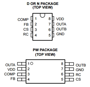
The UCC3808A family offers a variety of package options, temperature range options, and choice of undervoltage lockout levels. The family has UVLO thresholds and hysteresis options for off-line and battery powered systems. Thresholds are shown in the table below.
The UCC3808A is an enhanced version of the UCC3808 family. The significant difference is that the A versions feature an internal discharge transistor from the CS pin to ground, which is activated each clock cycle during the oscillator dead time. The feature discharges any filter capacitance on the CS pin during each cycle and helps minimize filter capacitor values and current sense delay.
block diagram
absolute maximum ratings over operating free-air temperature (unless otherwise noted)†
Supply voltage (IDD ≤ 10 mA) . . . . . . . . . . . . . . . . . . . . . . . . . . . . . . . . . . . . . . . . . . 15 V
Supply current . . . . . . . . . . . . . . . . . . . . . . . . . . . . . . . . . . . . . . . . . . . . . . . . . . . . . 20 mA
OUTA/OUTB source current (peak) . . . . . . . . . . . . . . . . . . . . . . . . . . . . . . . . . . . . . –0.5 A
OUTA/OUTB sink current (peak) . . . . . . . . . . . . . . . . . . . . . . . . . . . . . . . . . . . . . . . . 1.0 A
Analog inputs (FB, CS) . . . . . . . . . . . . . . . . . . . . . . –0.3 V to VDD 0.3 V, not to exceed 6 V
Power dissipation at TA = 25°C (N package) . . . . . . . . . . . . . . . . . . . . . . . . . . . . . . . . 1 W
Power dissipation at TA = 25°C (D package) . . . . . . . . . . . . . . . . . . . . . . . . . . . . . . 650 mW
Power dissipation at TA = 25°C (PW package) . . . . . . . . . . . . . . . . . . . . . . . . . . . . . 400 mW
Storage temperature, Tstg . . . . . . . . . . . . . . . . . . . . . . . . . . . . . . . . . . . . . . . –65°C to150°C
Junction temperature, TJ . . . . . . . . . . . . . . . . . . . . . . . . . . . . . . . . . . . . . . . . –55°C to 150°C
Lead temperature (soldering, 10 sec.) . . . . . . . . . . . . . . . . . . . . . . . . . . . . . . . . . . . . . 300°C
† Stresses beyond those listed under “absolute maximum ratings” may cause permanent damage to the device. These are stress ratings only, and functional operation of the device at these or any other conditions beyond those indicated under “recommended operating conditions” is not implied. Exposure to absolute-maximum-rated conditions for extended periods may affect device reliability.
† Currents are positive into, negative out of the specified terminal. Consult Packaging Section of the Power Supply Control Data Book (TI Literature Number SLUD003) for thermal limitations and considerations of packages.
Stock Offer (Hot Sell)
| Part no. | Quantity | Brand | D/C | Package |
| AT76C504-OZ160 | 145 | ATMEL | NEW | BGA |
| SA617D | 145 | PHILIPS | NEW | SOP-20 |
| LXT972ALC-A4 | 144 | INTEL | NEW | QFP |
| TMX320C6203BGLSX | 144 | TI | NEW | BGA |
| GM2126-BC | 143 | GENESIS | NEW | QFP |
| AD586LR-REEL | 142 | AD | NEW | SOP8 |
| TPS79325DBVR | 142 | TI | NEW | SOT23-5 |
| NLS045YFV-RA01 | 139 | NETLT | NEW | BGA |
| MIC4423ZN | 137 | MICREL | NEW | DIP8 |
| IRF7101TR | 136 | IR | NEW | SOP8 |
| MSM8939-1AA | 136 | QUALCOMM | NEW | BGA |
| SY10EL32VZG | 134 | MICREL | NEW | SOP8 |
| CS0100 | 133 | CAVIUM | NEW | BGA |
| MPC8343ZQAGD | 132 | EREESCAL | NEW | BGA |
| BPX48-Z | 130 | OSRAM | NEW | DIP-4 |
| L6221AD013TR | 127 | ST | NEW | SOP |
| ST62E28CF1 | 123 | ST | NEW | DIP28 |
| SY55855VKG | 122 | MICREL | NEW | SSOP10 |
| PEF4268TV1.2 | 120 | NEW | LQFP-64 | |
| XC3S500E-4FTG256C | 120 | XILINX | NEW | BGA |
| MAX4165EUK-T | 117 | MAXIM | NEW | SOT223 |
| NCP1570DR2 | 114 | ON | NEW | SOP8 |
| CY62128L-70SC | 112 | CYPREES | NEW | SOP32 |
| XC95108-7PQ160AEM | 112 | XILINX | NEW | QFP |
| S29GL512N11TAI010 | 110 | SPANSION | NEW | TSOP-56 |
| VSP9417B/C4 | 110 | MICRONAS | NEW | QFP |
| CY7C1354CV25-166AXC | 109 | CYPRESS | NEW | QFP |
| M29W010B90K1 | 108 | ST | NEW | PLCC |
| MHL19926 | 106 | FREESCALE | NEW | NI-360 |
| PCI1510PGE | 106 | TI | NEW | LQFP |


