Active Member
|
[China]

Address: Room 36B1-B2, Building C, Electronics Science & Technology Building Shennan Mid-Road, Shenzhen China
Contact name:Sharon Yang

Anterwell Technology Ltd. |

|
|
Stock Offer (Hot Sell)
| Part No. | Quantity | Brand | D/C | Package |
| M24512-WMN6TP | 7937 | ST | 16+ | SOP-8 |
| M24C02-WBN6P | 86000 | ST | 16+ | DIP-8 |
| M24C02-WMN6TP | 59000 | ST | 13+ | SOP-8 |
| M24C04-RMN6TP | 3696 | ST | 16+ | SOP-8 |
| M24C04-WBN6P | 16899 | ST | 14+ | DIP-8 |
| M24C04-WMN6TP | 122000 | ST | 10+ | SOP-8 |
| M24C08-WMN6TP | 74000 | ST | 11+ | SOP-8 |
| M24C32-WMN6TP | 73000 | ST | 13+ | SOP-8 |
| M24C64-WMN6TP | 94000 | ST | 12+ | SOP-8 |
| M24M01-RMN6TP | 3725 | ST | 16+ | SOP-8 |
| M25P128-VMF6TPB | 3811 | MICRON | 15+ | SOP-16 |
| M25P40-VMN6TPB | 19084 | MICRON | 16+ | SOP-8 |
| M27C512-10F1 | 4015 | ST | 14+ | DIP |
| M27C512-12F1 | 9061 | ST | 16+ | DIP |
| M28W320CT70N6 | 8447 | STM | 04+ | TSOP-48 |
| M29W160EB70N6E | 5726 | STM | 12+ | TSSOP-48 |
| M29W640GB70NA6E | 4271 | ST | 14+ | TSSOP |
| M30620FCPFP#U5C | 2021 | RENESAS | 08+ | QFP |
| M35080-WMN3TP | 3105 | STM | 16+ | SOP-8 |
| M41T00M6E | 15100 | ST | 11+ | SOP-8 |
| M41T56M6F | 18066 | ST | 11+ | SOP-8 |
| M41T81M6F | 6308 | ST | 13+ | SOP-8 |
| M48T02-150PC1 | 3063 | ST | 16+ | DIP-24 |
| M48T35AV-10PC1 | 3160 | ST | 16+ | DIP |
| M48T58-70PC1 | 1980 | ST | 14+ | DIP |
| M48T86PC1 | 6681 | ST | 16+ | DIP |
| M5218AL | 10864 | RENESAS | 14+ | ZIP-8 |
| M54581P | 6591 | MIT | 16+ | DIP-18P |
| M57774 | 2065 | MITSUBISH | 13+ | SMD |
| M5L8251AP-5 | 3953 | MIT | 13+ | DIP-28 |
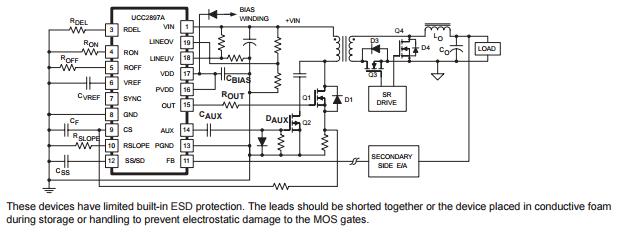
UCC2897A
ADVANCED CURRENT-MODE ACTIVE CLAMP PWM CONTROLLER
FEATURES
APPLICATIONS
DESCRIPTION
The UCC2897A PWM controller simplifies implementation of the various active clamp/reset and synchronous rectifier switching power topologies.
The UCC2897A is a peak current-mode, fixedfrequency, high-performance pulse width modulator. It includes the logic and the drive capability for the P-channel auxiliary switch along with a simple method of programming the critical delays for proper active clamp operation.
Features include an internal programmable slope compensation circuit, precise DMAX limit, and a synchronizable oscillator with an internal timing capacitor. An accurate line monitoring function also programs the converter’s ON and OFF transitions with regard to the bulk input voltage, VIN.
The UCC2897A adds a second level hiccup mode current sense threshold, bi-directional synchronization and input overvoltage protection functionalities. The UCC2897A is offered in 20-pin TSSOP (PW) and 20-pin QFN (RGP) package.
ABSOLUTE MAXIMUM RATINGS
over operating free-air temperature range unless otherwise noted(1)
| Line input voltage, VIN | 120 | V | |
| Supply voltage, VDD | (IDD < 10 mA) | 116.5 | V |
| Analog inputs | FB, CS, SYNC, LINEOV, LINEUV | −0.3 to (VREF + 0.3) | V |
| Output source current (peak), IO_SOURCE | OUT, AUX | 2.5 | A |
| Output sink current (peak), IO_SINK | -2.5 | ||
| Operating junction temperature range, TJ | −55 to 150 | °C | |
| Storage temperature, Tstg | −65 to 150 | °C | |
| ESD rating | Human body model, (HBM) | 2000 | V |
| Charged device model (CDM) | 500 | ||
| Lead temperature, Tsol, 1,6 mm (1/16 inch) from case for 10 seconds | 300 | °C | |
(1) Stresses beyond those listed under “absolute maximum ratings” may cause permanent damage to the device. These are stress ratings only, and functional operation of the device at these or any other conditions beyond those indicated under “recommended operating conditions” is not implied. Exposure to absolute-maximum-rated conditions for extended periods may affect device reliability. All voltages are with respect to GND. Currents are positive into and negative out of, the specified terminal.
TYPICAL APPLICATION DIAGRAM