

Active Member
|
[China]

Address: Room 36B1-B2, Building C, Electronics Science & Technology Building Shennan Mid-Road, Shenzhen China
Contact name:Sharon Yang

Anterwell Technology Ltd. |

|
|
General Description
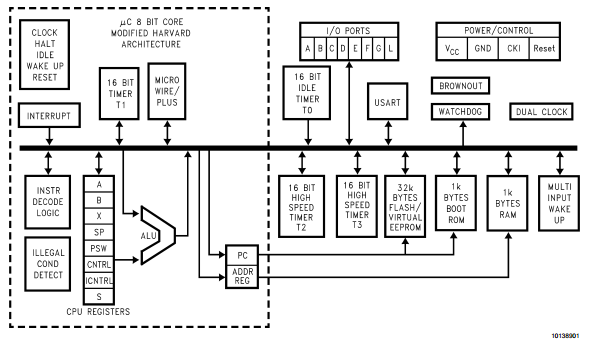
The COP8SBR9/SCR9/SDR9 Flash based microcontrollers are highly integrated COP8™ Feature core devices, with 32k Flash memory and advanced features including Virtual EEPROM, High Speed Timers, USART, and Brownout Reset. This single-chip CMOS device is suited for applications requiring a full featured, in-system reprogrammable controller with large memory and low EMI. The same device is used for development, pre-production and volume production with a range of COP8 software and hardware development tools.
KEY FEATURES
►32 kbytes Flash Program Memory with Security Feature
► Virtual EEPROM using Flash Program Memory
►1 kbyte volatile RAM
►USART with on chip baud generator
► 2.7V–5.5V In-System Programmability of Flash
► High endurance - 100k Read/Write Cycles
►Superior data retention - 100 years
►Dual Clock Operation with HALT/IDLE Power Save Modes
Block Diagram
Absolute Maximum Ratings
If Military/Aerospace specified devices are required, please contact the National Semiconductor Sales Office/ Distributors for availability and specifications.
Supply Voltage (VCC) 7V 
Voltage at Any Pin −0.3V to VCC +0.3V
Total Current into VCC Pin (Source) 200 mA
Total Current out of GND Pin (Sink) 200 mA
Storage Temperature Range −65˚C to +140˚C
ESD Protection Level 2 kV (Human Body Model)
FUNCTIONAL DESCRIPTION
The organization of the ISP feature consists of the user flash program memory, the factory boot ROM, and some registers dedicated to performing the ISP function. See Figure 13 for a simplified block diagram. The factory installed ISP that uses MICROWIRE/PLUS is located in the Boot ROM. The size of the Boot ROM is 1K bytes and also contains code to facilitate in system emulation capability. If a user chooses to write his own ISP routine, it must be located in the flash program memory


