Active Member
|
[China]

Address: UNIT04,7/F BRIGHT WAY TOWER NO.33 MONG KOK RD KL HONGKONG CHINA
Contact name:Richard

Garant Optima Co., Ltd |
|
|
JM-S2TR31-3-10-SDI SFP optical transceiver module includes two parts--the transmitterJM-S2T31-3-10-SDI and the receiver JM-S2R31-3-10-SDI
Features Description
1,For JM-S2T31-3-10-SDI part,
>>1310nm DFB Laser diode transmitter,
For JM-S2R31-3-10-SDI part,
>>1310nm InGaAs PIN photodiode receiver
2,Transceiver unit with independent
3,SMPTE 297-2006 compatible
4,Robust error-free transmission of signals from 50Mbps to 3Gbps with up to 10km single-mode fiber
5,Maximum distance of 10km under worst-case conditions and 3Gbps video pathological signals
6,Supports video pathological patterns for SD-SDI,HD-SDI and 3G-SDI
7,SFP Package.Hot-pluggable
8,Metal enclosure for lower EMI
9,+3.3V single power supply.
10,Two independent laser disable pins
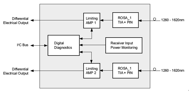
11,Digital diagnostics and control via I²C interface, including:
12,Monitoring laser bias current, average output power, supply voltage and temperature
13,Alarm reporting when transmitter is at fault
14,Module ID polling
15,Compliant ROHS and lead free
Applications
SMPTE 297-2006 compatible electrical-to-optical interfaces
Descriptions
The JM-S2T31-3-10-SDI is a dual channel optical transmitter module designed to transmit optical serial digital signals as defined in SMPTE 297-2006. It is specifically designed for robust performance in the presence of SDI pathological patterns for SMPTE 259M, SMPTE 344M, SMPTE 292M and SMPTE 424M serial rates.
The JM-S2R31-3-10-SDI is a dual channel optical receiver module designed to convert optical serial digital signals to electrical serial digital signals as defined in SMPTE 297-2006 . It is specifically designed for robust performance in the presence of SDI pathological patterns for SMPTE 259M, SMPTE 292M and SMPTE 424M serial rates.
Functional Block Diagram

Pin Description
JM-S2T31-3-10-SDI Pin Out Diagram

JM-S2R31-3-10-SDI Pin Out Diagram
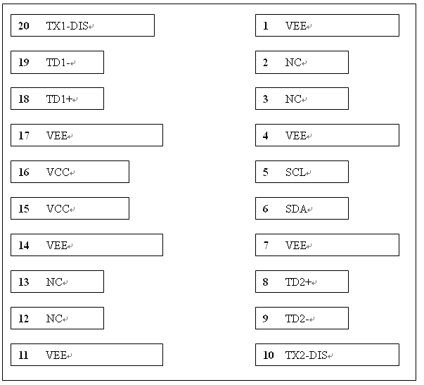
JM-S2T31-3-10-SDI Pin Function Definition
| Pin# | Name | Description | Notes |
| 1 | VEE | Ground | - |
| 2 | NC | No Connection | - |
| 3 | NC | No Connection | - |
| 4 | VEE | Ground | - |
| 5 | SCL | I²C Clock | - |
| 6 | SDA | I²C Data | - |
| 7 | VEE | Ground | - |
| 8 | TD2+ | Transmit Data In | Note 1 |
| 9 | TD2- | Inv. Transmit Data In | Note 1 |
| 10 | TX2-DIS | Transmitter Disable | Note 2, Module disables on high or open |
| 11 | VEE | Ground | - |
| 12 | NC | No Connection | - |
| 13 | NC | No Connection | - |
| 14 | VEE | Ground | - |
| 15 | VCC | Transmitter Power | Note 3, 3.3V± 5% |
| 16 | VCC | Transmitter Power | Note 3, 3.3V± 5% |
| 17 | VEE | Ground | - |
| 18 | TD1+ | Transmit Data In | Note 1 |
| 19 | TD1- | Inv. Transmit Data In | Note 1 |
| 20 | TX2-DIS | Transmitter Disable | Note 2, Module disables on high or open |
Note:
1. TD-/+: These are the differential transmitter inputs. They are AC-coupled, differential lines with 100Ω differential termination inside the module.
2. TX-disable is an input that is used to shut down the transmitter optical output. It is pulled up within the module with a 4.7–10 KΩ resistor. Its states are:
Low (0 – 0.8V): Transmitter on
(>0.8, < 2.0V): Undefined
High (2.0 – 3.465V): Transmitter Disabled
Open: Transmitter Disabled
3. VCC is the transmitter power supplies. It is defined as 3.3V ±5% at the SFP connector pin. Maximum supply current is 300mA. Recommended host board power supply filtering is shown below. Inductors with DC resistance of less than 1Ω should be used in order to maintain the required voltage at the SFP input pin with3.3V supply voltage. When the recommended supply filtering network is used, hotplugging of the SFP transceiver module will result in an inrush current of no more than 30 mA greater than the steady state value.
JM-S2R31-3-10-SDI Pin Function Definition
| Pin# | Name | Description | Notes |
| 1 | VEE | Ground | - |
| 2 | RD2- | Inv. Received Data Out | Note 1 |
| 3 | RD2+ | Receiver Data out | Note 1 |
| 4 | VEE | Ground | - |
| 5 | SCL | I²C Clock | - |
| 6 | SDA | I²C Data | - |
| 7 | VEE | Ground | - |
| 8 | NC | No Connection | - |
| 9 | NC | No Connection | - |
| 10 | NC | No Connection | - |
| 11 | VEE | Ground | - |
| 12 | RD1- | Inv. Received Data Out | Note 1 |
| 13 | RD1+ | Receiver Data out | Note 1 |
| 14 | VEE | Ground | - |
| 15 | VCC | Receiver Power Supply | Note 2, 3.3V± 5% |
| 16 | VCC | Receiver Power Supply | Note 2, 3.3V± 5% |
| 17 | VEE | Ground | - |
| 18 | NC | No Connection | - |
| 19 | NC | No Connection | - |
| 20 | NC | No Connection | - |
Note:
1. RD-/+: These are the differential receiver outputs. They are AC coupled 100Ω differential lines which should be terminated with 100Ω (differential) at the user SERDES. The AC coupling is done inside the module and is thus not required on the host board.
2. VCC is the receiver power supplies. It is defined as 3.3V ±5% at the SFP connector pin. Maximum supply current is 300mA. Recommended host board power supply filtering is shown below. Inductors with DC resistance of less than 1Ω should be used in order to maintain the required voltage at the SFP input pin with3.3V supply voltage. When the recommended supply filtering network is used, hotplugging of the SFP transceiver module will result in an inrush current of no more than 30 mA greater than the steady state value.
Recommended Host Board Supply Filtering

Optical Connector Requirements
Dual LC connector with PC/UPC polish is required for each port.
Performance Specifications
Absolute Maximum Ratings
| Parameter | Symbol | Min. | Max. | Unit |
| Storage Temperature | TST | -40 | +85 | ℃ |
| Operating case Temperature | Tcase | -20 | +85 | ℃ |
| Input Voltage | - | GND | VCC | V |
| Power Supply Voltage | VCC-VEE | -0.5 | +3.6 | V |
| Parameter | Symbol | Min. | Max. | Unit |
| Power Supply Voltage | VCC | +3.1 | +3.5 | V |
| Operating Temperature | To | 0 | +70 | ℃ |
Transmitter E-O characteristics
| Parameter | Symbol | Min. | Typ. | Max. | Unit | Note |
| Bit Rate | BR | 50 | - | 3000 | Mbps | - |
| Center Wavelength | lp | l-6 | l | l+7.5 | nm | T=0~ +70℃ l:CWDM |
| Spectral Width (-20dB) | Dl | - | - | 1 | nm | - |
| Side Mode suppression Ratio | SMSR | 30 | - | - | dB | - |
| Average Optical Output Power | Po | -8 | -5 | -3 | dBm | - |
| Extinction Ratio | ER | 7 | - | - | dB | - |
| Power Supply Current | ICC | - | 70 | 180 | mA | - |
| Transmitter Enable Voltage | VEN | 0 | - | 0.8 | - | - |
| Transmitter disable Voltage | VD | 2.0 | - | VCC | V | - |
| Data Inputs Voltage | VPP | 300 | 800 | 1600 | mV | - |
| Optical Rise Time (20%~80%) | Tr | - | 105 | 165 | ps | SMPTE424M 2.97Gbps |
| - | 170 | 270 | ps | SMPTE 292M 1.485Gbps | ||
| - | 300 | 800 | ps | SMPTE 259M 270Mbps | ||
| Optical Fall Time (80%~20%) | Tf | - | 120 | 180 | ps | SMPTE 424M 2.97Gbps |
| - | 170 | 270 | ps | SMPTE 292M 1.485Gbps | ||
| - | 300 | 800 | ps | SMPTE 259M 270Mbps | ||
Optical Signal Intrinsic Jitter |
- | - | 45 | 70 | ps
| SMPTE 424M 2.97Gbps |
| - | 60 | 100 | ps | SMPTE 292M 1.485Gbps | ||
| - | 110 | 180 | ps | SMPTE 259M 270Mbps |
Receiver O-E characteristics
| Parameter | Symbol | Min. | Typ. | Max. | Unit | Note |
| Bit Rate | BR | 50 | - | 3000 | Mbps | - |
| Wavelength | l | 1260 | - | 1620 | nm | - |
| Saturation | Ps | 0 | - | - | dBm | - |
| LOS Asserted | - | -35 | - | - | dBm | - |
| LOS De-Assert | - | - | - | -22 | dBm | - |
| LOS Hysteresis | - | - | 3 | - | dB | - |
| LOS LOW voltage | VLout | 0 | - | 0.8 | V | - |
| LOS HIGH voltage | VHout | 2.0 | - | Vcc | V | - |
Sensitivity for SMPTE 259M 143-360Mbps | - | - | -22 | -20 | dBm | Pathological |
| - | -24 | -22 | dBm | PRBS | ||
Sensitivity for SMPTE 292M 1.485Gbps | - | - | -22 | -20 | dBm | Pathological |
| - | -24 | -22 | dBm | PRBS | ||
Sensitivity for SMPTE 424M 2.97Gbps |
- | - | -20 | -18 | dBm | Pathological |
| - | -22 | -20 | dBm | PRBS | ||
| Data Outputs Voltage | Vpp | 400 | 800 | 1000 | mV | - |
| Input Power Monitoring Accuracy | -1 | +1 | dB | - |
Note: The sensitivity specification refers to the input power levels for BER = 1E-12 against PRBS 2^23-1.
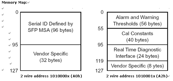
EEPROM Section
Serial Interface
The optical transmitter and receiver contains an EEPROM. It provides access to sophisticated identification information that describes the transmitter’s capabilities, standard interfaces, manufacturer, and other information. The serial interface uses the 2-wire serial CMOS EEPROM protocol defined for the ATMEL AT24C01A/02/04 family of components. When the serial protocol is activated, the host generates the serial clock signal (SCL). The positive edge clocks data into those segments of the EEPROM that are not write protected within the transmitter. The negative edge clocks data from the transmitter. The serial data signal (SDA) is bi-directional for serial data transfer. The host uses SDA in conjunction with SCL to mark the start and end of serial protocol activation. The memories are organized as a series of 8-bit data words that can be addressed individually or sequentially.
The Module provides diagnostic information about the present operating conditions. The transmitter generates this diagnostic data by digitization of internal analog signals. Calibration and alarm/warning threshold data is written during device manufacture. Transmitted power monitoring, bias current monitoring, supply voltage monitoring and temperature monitoring all are implemented. The diagnostic data are raw A/D values and must be converted to real world units using calibration constants stored in EEPROM locations 56 – 95 at wire serial bus address A2h. The digital diagnostic memory map specific data field define as following.
JM-S2T31-3-10-SDI Typical application Circuit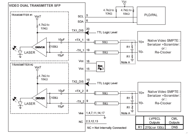
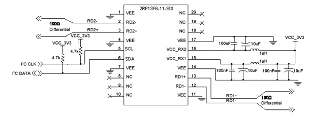
JM-S2R31-3-10-SDI Typical application Circuit
Recommended Circuit
Note: 4.7K ohms﹤RES﹤10K ohms
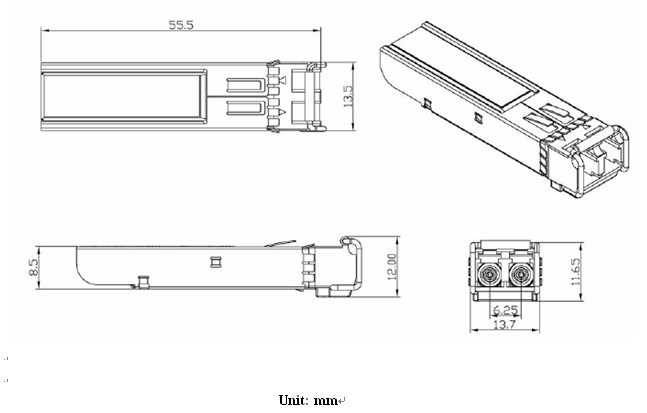
Package information